Selected Recent Publications
Complete list avilable @ Dr. Ganapathy's Google Scholar page
Atomic Origins of Phase Transition in Doped VO2 Nanowires
Tuning the metal-insulator transition in VO2 with tungsten doping reveals atomistic insights into phase behavior. Our findings show that localized strain from dopants accelerates phase transitions, offering a pathway to engineer ultrafast electronic switches and electro-optical sensors.
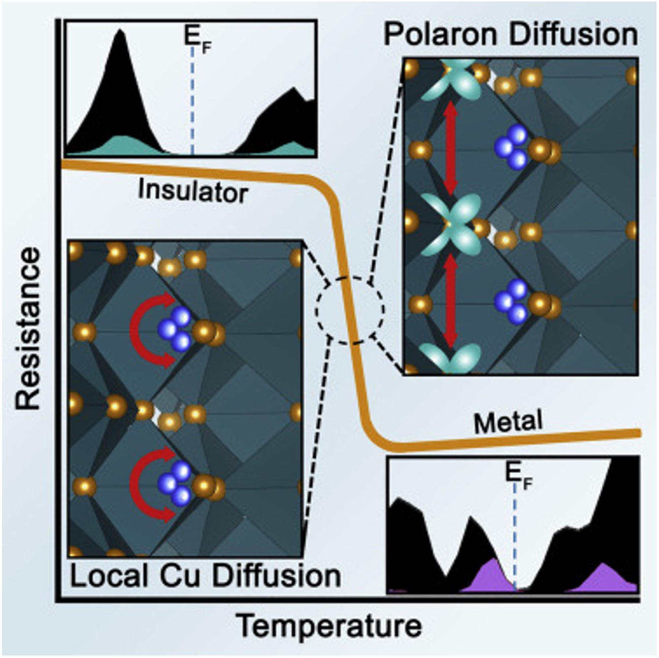
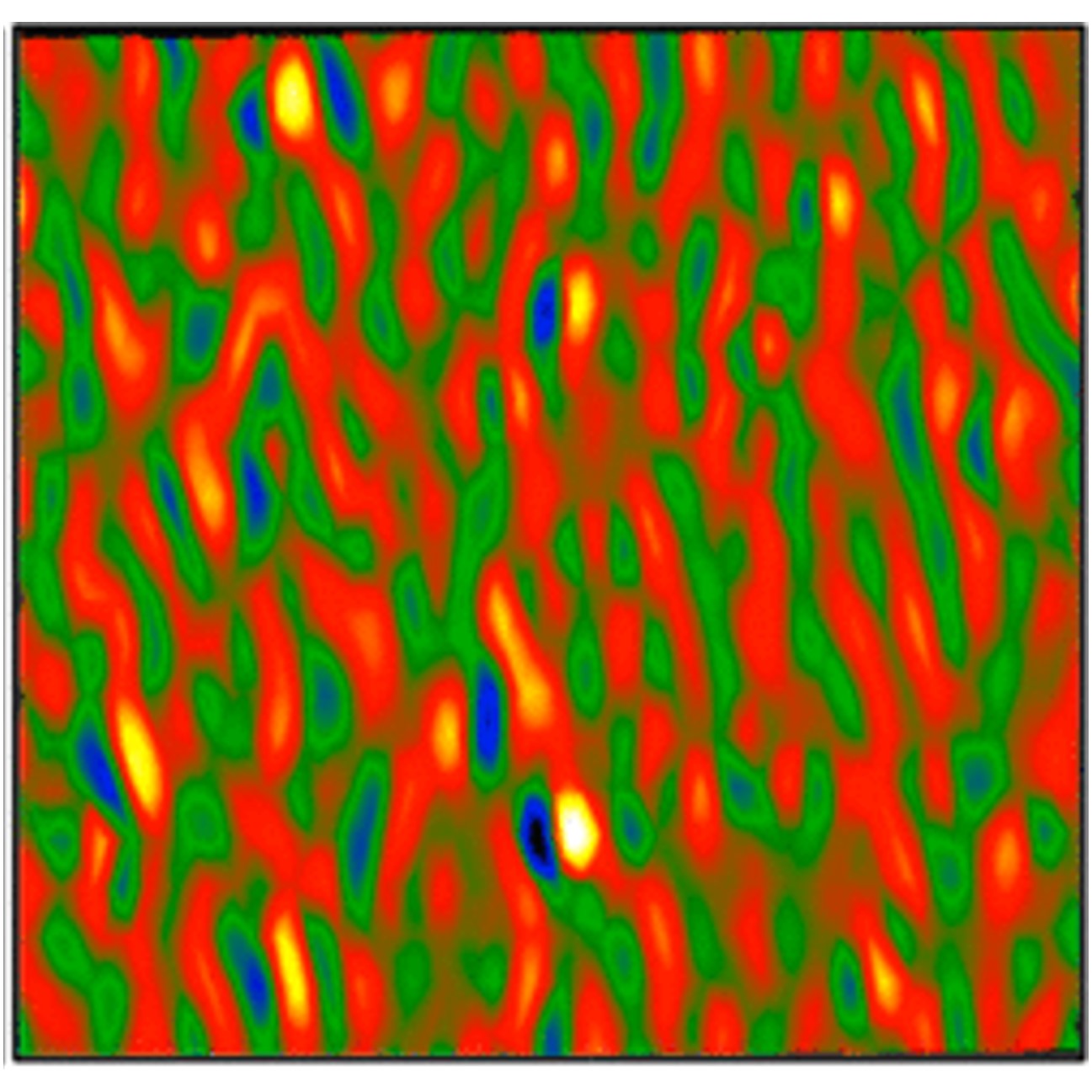
Polaron Oscillation and Cation Shuttling in β′-CuxV2O5
ransition metal oxides, like β′-CuxV2O5, offer energy-efficient alternatives to silicon by mimicking neural spiking behavior. Our study shows that Cu ion motion and polaron oscillation drive metal-insulator transitions, paving the way for advanced neuromorphic computing applications.
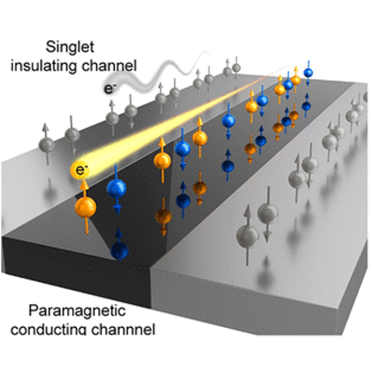
Magneto-Electronic Switchable Molecular Electronic Crystal
Electrically driven phase transitions in molecular crystals, like K-TCNQ, open doors to quantum sensing and information technology. Our findings highlight dynamic magneto-electric switching, promising a path toward molecular-based memory and switching devices.
- News item: How can AI be more energy-efficient? UB researchers look to human brain for inspiration (2025). [link]
- N. Kumar, N. Jerla, J. Ponis, S. Banerjee, G. Sambandamurthy, “Low-Frequency Noise and Resistive Switching in β-Na0.33V2O5,”(2025). under review.
- G. Agbeworvi, N. Kumar, J.D. Ponis, S. Hariyani, N. Jerla, F. Jardali, J. Li, W. Zaheer, J.V. Handy, J.R. Ayala, C. Jaye, C. Weiland, D.A. Fischer, P.J. Shamberger, J. Guo, R.S. Williams, G. Sambandamurthy, S. Banerjee, “An Atom-Precise Approach for Introducing Weak Disorder in First-Order Phase Transitions to Stabilize Broad-Frequency Neuromorphic Oscillators,” (2025). under review.
- N. Kumar, J.E. Han, K. Beckmann, N. Cady, G. Sambandamurthy, “Noise Spectroscopy and Electrical Transport in NbO2 Memristors with Dual Resistive Switching,” Advanced Electronic Materials 11 (9), 2400877 (2025). [link]
- D. Kaushik, N. Kumar, R. Srivastava, G. Sambandamurthy, “Zeolitic-Imidazole Framework (ZIF-8) Based Memristors for Neuromorphic Computing,” Physical Review Applied 23, 064059 (2025). [link]
- J. Ponis, N. Jerla, G. Agbeworvi, S. Perez-Beltran, N. Kumar, K. Ashen, J. Li, E. Wang, M. A. Smeaton, F. Jardali, S. Chakraborty, P. J. Shamberger, K. L. Jungjohann, C. Weiland, C. Jaye, L. Ma, D. Fischer, J. Guo, G. Sambandamurthy, X. Qian, S. Banerjee, “Atomistic Origins of Conductance Switching in an ε-Cu0.9V2O5 Neuromorphic Single Crystal Oscillator,” Journal of the American Chemical Society 146 (50), 34536–34550 (2024). [link]
- Z. Shi, L. Zhu, P. M. Marley, K. Farley, S. Banerjee, G. Sambandamurthy, “The dynamics of pinned charge density wave in NbSe3 nanoribbons revealed by noise spectroscopy,” New Journal of Physics 26 (12), 123002 (2024). [link]
- Y. Hu, D. Adhikari, X. Dong, A. H. Ali, P. Zhang, G. Sambandamurthy, S. Ren, “High-endurance magneto-electronic switchable molecular electronic crystal,” Nano Letters 22 (7), 3151 (2022). [link]
- Y. Hu, D. Adhikari, A. Tan, X. Dong, T. Zhu, X. Wang, T. Mitchell, Z. Yao, N. Dasenbrock-Gammon, E. Snider, R. Dias, C. Huang, R. Kim, I. Neuhart, A. H. Ali, J. Zhang, H. Bechtel, M. Martin, S. Gilbert Corder, Y. Huang, F. Hu, Z. Li, J. Armstrong, J. Wang, M. Liu, J. Benedict, E. Zurek, G. Sambandamurthy, J. Grossman, P. Zhang, S. Ren, “Laser-induced Cooperative Transition in Molecular Electronic Crystal,” Advanced Materials 33 (39), 2103000 (2021). [link]
- A. Parija, J. V. Handy, J. L. Andrews, J. Wu, L. Wangoh, S. Singh, C. Jozwiak, A. Bostwick, E. Rotenberg, W. Yang, S. C. Fakra, M. Al-Hashimi, G. Sambandamurthy, L. F. J. Piper, R. Stanley Williams, D. Prendergast, S. Banerjee, “Metal-Insulator Transitions in β′-CuxV2O5 Mediated by Polaron Oscillation and Cation Shuttling,” Matter 2, 1166 (2020). [link]
- C. Kilcoyne, Ahmed Ali, A. Alsaqqa, A. A. Rahman, L. Whittaker-Brooks, and G. Sambandamurthy, “Gate-tunable transport characteristics of single nanowire transistors of Bi2S3,” Solid State Communications 270, 135 (2018). [link]
- A. Alsaqqa, S. Singh, S. Middey, M. Kareev, J. Chakhalian, G. Sambandamurthy, “Phase coexistence and dynamical behavior in NdNiO3 ultrathin films,” Physical Review B 95, 125132 (2017). [link]
- S. Singh, T. A. Abtew, G. Horrocks, P. M. Marley, A. A. Stabile, S. Banerjee, P. Zhang, and G. Sambandamurthy, “Selective electrochemical reactivity of rutile VO2 towards the suppression of metal-insulator transition,” Physical Review B 93, 125132 (2016). [link]
- A. Stabile, S. Singh, T.-l. Wu, L. Whittaker, S. Banerjee, and G. Sambandamurthy, “Separating electric field and thermal effects across the metal-insulator transition in vanadium oxide nanobeams,” Applied Physics Letters 107, 013503 (2015). [link]
- S. Singh, G. Horrocks, P. M. Marley, Z. Shi, S. Banerjee, and G. Sambandamurthy, “Proliferation of metallic domains caused by inhomogeneous heating near the electrically-driven transition in VO2 nanobeams,” Physical Review B 92, 155121 (2015). [link]
- H. Asayesh-Ardakani, A. Nie, P. M. Marley, S. Singh, F. Mashayek, G. Sambandamurthy, K.-b. Low, R. F. Klie, S. Banerjee, G. M. Odegard, R. Shahbazian-Yassar, “Atomic origins of the Monoclinic-Tetragonal phase transition in doped VO2 nanowires,” Nano Letters 15, 7179-7188 (2015). [link]
- J. B. Hatch, L. Whittaker-Brooks, T. L. Wu, G. Long, H. Zeng, G. Sambandamurthy, S. Banerjee, H. Luo, “Intermediate metallic phase in VO2 observed with scanning tunneling spectroscopy,” Physical Chemistry Chemical Physics 16, 14183-14188 (2014). [link]
- W. Liu, L. Pan, J. Wen, M. Kim, G. Sambandamurthy, and N. P. Armitage, “Microwave Spectroscopy Evidence of Superconducting Pairing in the Magnetic-Field-Induced Metallic State of InOx Films at Zero Temperature,” Physical Review Letters 111, 067003 (2013). [link]
- S. Misra, L. Urban, M. Kim, G. Sambandamurthy, and A. Yazdani, “Measurements of the Magnetic-Field-Tuned Conductivity of Disordered Two-Dimensional Mo43Ge57 and InOx Superconducting Films: Evidence for a Universal Minimum Superfluid Response,” Physical Review Letters 110, 037002 (2013). [link]
- P. Marley, A. Stabile, C. P. Kwan, S. Singh, G. Sambandamurthy, and S. Banerjee, “Charge Disproportionation, Charge Ordering, and Voltage-Induced Metal-Insulator Transitions in β-PbxV2O5 Nanowires,” Advanced Functional Materials 23, 153 (2013). [link]
- T.-l. Wu, A. Stabile, C. J. Patridge, S. Banerjee, and G. Sambandamurthy, “Electrically driven Metal-Insulator Transition in nanowires of a vanadium oxide bronze,” Applied Physics Letters 101, 163502 (2012). [link]
- A. Stabile, L. Whittaker, T.-l. Wu, P. Marley, S. Banerjee, and G. Sambandamurthy, “Synthesis, characterization, and finite size effects on electrical transport of nanoribbons of charge density wave conductor NbSe3,” Nanotechnology 22, 485201 (2011). [link]
- L. Whittaker, T.-l. Wu, A. Stabile, G. Sambandamurthy, and S. Banerjee, “Single-Nanowire Raman Microprobe Studies of Temperature- and Voltage-Induced Metal—Insulator Transitions of WxV1-xO2 Nanowires,” ACS Nano 5, 8861 (2011). [link]
- T.-l. Wu, L. Whittaker, S. Banerjee, and G. Sambandamurthy, “Temperature and voltage driven tunable metal-insulator transition in individual WxV1-xO2 nanowires,” Physical Review B 83, 073101 (2011). [link]
- C. J. Patridge, T.-l. Wu, C. Jaye, B. Ravel, E. Takeuchi, D. A. Fischer, G. Sambandamurthy, and S. Banerjee, “Synthesis, Characterization and Observation of Massive Metal-Insulator Transitions in Nanowires of a Non-Stoichiometric Vanadium Oxide Bronze,” Nano Letters 10, 2448 (2010). [link]
- Han Zhu, G. Sambandamurthy, Yong P. Chen, Pei-Hsun Jiang, L. W. Engel, D. C. Tsui, L. N. Pfeiffer, and K. W. West, “Pinning mode resonance of a Skyrme crystal near Landau level filling of n = 1,” Physical Review Letters 104, 226801 (2010). [link]
- Han Zhu, G. Sambandamurthy, L. W. Engel, D. C. Tsui, L. N. Pfeiffer, and K. W. West, “Pinning mode resonances of 2D electron stripe phases: Effect of in-plane magnetic field,” Physical Review Letters 102, 136894 (2009). [link]
- G. Sambandamurthy, R. M. Lewis, Han Zhu, Y. P. Chen, L. W. Engel, D. C. Tsui, L. N. Pfeiffer, and K. W. West, “Observation of Pinning Mode of Stripe Phases of 2D Systems in High Landau Levels,” Physical Review Letters 100, 256801 (2008). [link]
- R. Crane, N. Peter Armitage, A. Johansson, G. Sambandamurthy, D. Shahar, and G. Gruner, “Fluctuations, dissipation and non-universal superfluid jumps in two-dimensional superconductors,” Physical Review B 75, 094506 (2007). [link]
- Y. P. Chen, G. Sambandamurthy, Z. H. Wang, R. M. Lewis, L. W. Engel, D. C. Tsui, P. D. Ye, L. N. Pfeiffer, and K. W. West, “Melting of a 2D quantum electron solid,” Nature Physics 2, 452 (2006). [link]
- A. Johansson, G. Sambandamurthy, D. Shahar, N. Jacobson, and R. Tenne, “Nanowire acting as a superconducting quantum interference device,” Physical Review Letters 95, 116805 (2005). [link]
- G. Sambandamurthy, L. W. Engel, A. Johansson, E. Peled, and D. Shahar, “Experimental evidence for a collective insulating state in two-dimensional superconductors,” Physical Review Letters 94, 017003 (2005). [link]
- G. Sambandamurthy, L. W. Engel, A. Johansson, and D. Shahar, “Superconductivity-related insulating behavior,” Physical Review Letters 92, 107005 (2004). [link]