CSE 493/593 Fall 2024
Cadence Tutorial
This
tutorial assumes that you have started up Cadence and the CIW and Library
Manager window are open. If they are not, please refer to the Cadence
Setup page for this procedure.
Creating
New Library:
All designs related to a project are stored in a library.
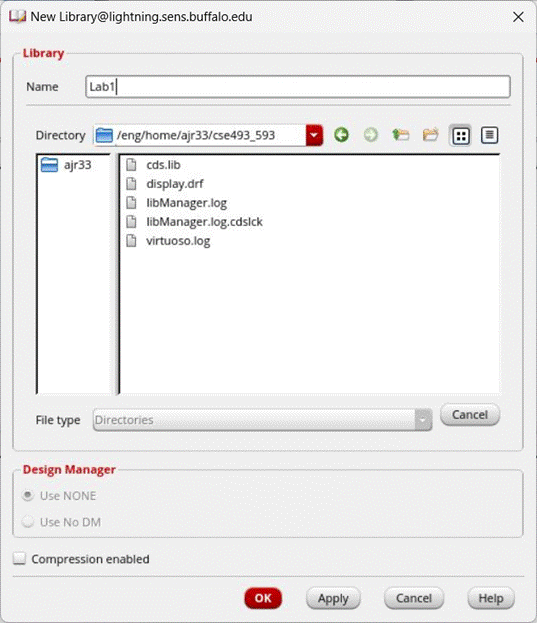
To create a new library from the Library Manager, click on File -> New ->
Library. In the New Library window, type Lab1 as the name of
the library and click OK:
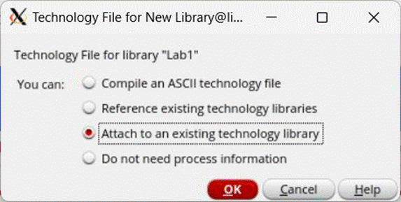
In the
Technology File for New Library window, select attach to existing technology
library and click OK:
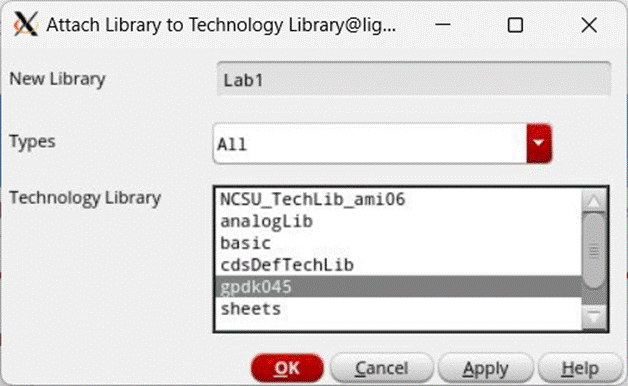
In the
next window, select gpdk045 and click OK
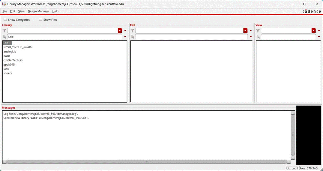
Now the
library Lab1 is created.
Creating new schematic design
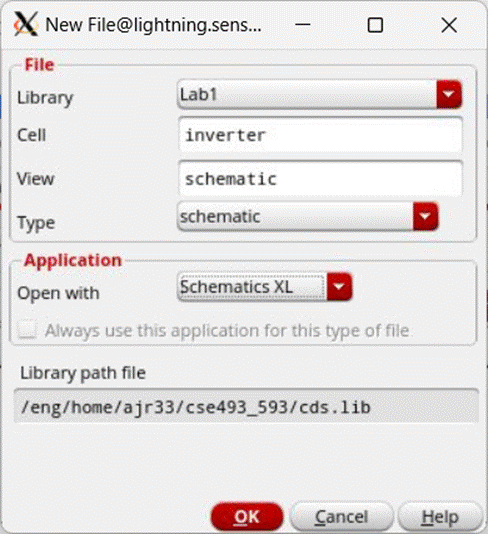
In the
Library Manager window, click on File -> New -> Cell View
In the
New File window, make sure that the library is set to Lab1
Name
the cell inverter
Set
type to schematic. The view should automatically be named to schematic.
Set the
application to open with to Schematics XL.
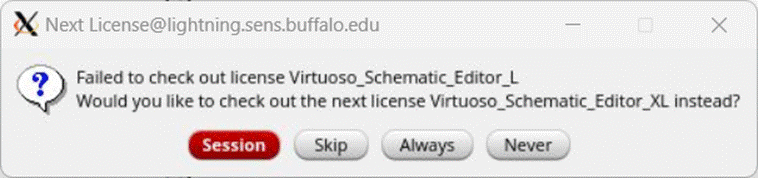
If the Next
License window appears, click Session or Always. This will happen if you select
Schematics L application instead.
The
Virtuoso Studio Schematic XL tool appears, as shown below:
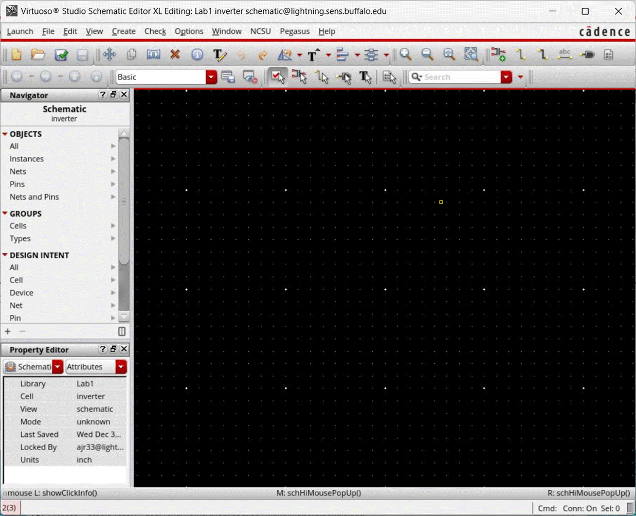
At this
point, you have created a library called Lab1 and a cell inside it, called inverter.
Now the design process can be started. For a full custom design, the process
begins by creating a schematic. Then we simulate this design to verify the
correctness of its functionality. Only after this is done, is the layout of the
design performed.
Here
are some hot keys in the schematic composer:
- i: Add instances
- m: Move object
- q: Edit object properties (Q for
editing cellview properties)
- w: Add wires
- p: Add a pin
- l: Label a wire
- z: Zoom in
- Z: Zoom out by 2X
- f: fit the schematic in your schematic
window
Now, we
put down the design of the inverter in the Schematic Editor window. The
Inverter consists of a NMOS and PMOS transistor with appropriately connected
gate, drain and source terminals. The transistors and the input signal sources
are instantiated and connected in the schematic editor. To instantiate a
NMOS transistor :
Create
Instance:
In the
schematic window, click on Create->Instance (or type i). The Add instance dialogue box appears together with the
Component Browser dialog box. (In case the Component Browser does not appear,
click on browse in the "Add Instance" dialog box to start it.)
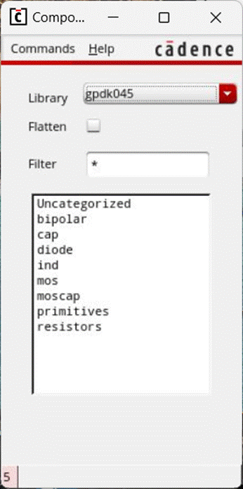
In the
Component Browser window, Click on Library and choose gpdk045. Click on mos and choose nmos1v as your NMOS device. To place
the instance, activate the schematic window and click the left mouse button to
put the instance at the place desired.
You can
also use the Add Instance window to select the device to place.
Note in
Cadence Virtuoso schematic composers and layout editors, a command will not
terminate unless the user cancels it, or the user starts a new command. In this
case, you can see another instance is ready to be placed right after you placed
the first instance. To terminate the current operation (which is "add
instance" in this case), press ESC key on the keyboard. In fact, you can
always cancel the current operation in schematic or layout editors by pressing
ESC key.
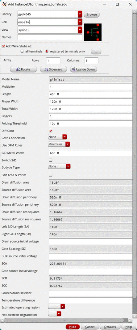
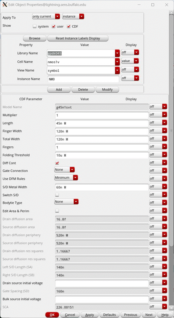
Edit
Object Properties:
Now, we
set the length and width of the NMOS transistor that is instantiated. To do
this, select the object (NMOS transistor) by clicking on it and then go to Edit
-> properties -> Object... (or by typing q). An object
properties editing form will pop up. In this form, make the NMOS Length 45n,
Finger Width 120n, Total Width 120n & Fingers 1.
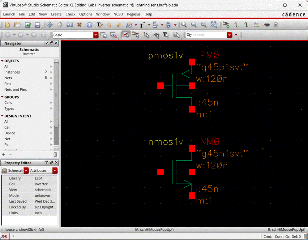
Repeat
the Create Instance procedure for a PMOS transistor using pmos1v and set
its Length to 45n, Finger Width 120n, Total Width 120n
& Fingers 1. The schematic should look similar to
this:
Wiring up:
To connect
the PMOS and NMOS devices or any electrical device, click on Create ->
Wire(narrow) in the schematic window (or type w). Click at the terminal where
the wire starts and click at the terminal where the wire ends, a wire will be
automatically added. If you are not satisfied with the automatic wiring, you
can remove the wire and reroute it manually. This time, instead of clicking at
the terminal where the wire ends directly, you can click the left mouse button
whenever you want to change the wire direction.
If you want to stop the wire somewhere instead of connecting it to a terminal,
double click your left mouse button and a dangling wire is created. In general
dangling wire should be avoided, however, in some cases (like you want to label
this wire or add a pin to this wire), a dangling wire makes sense.
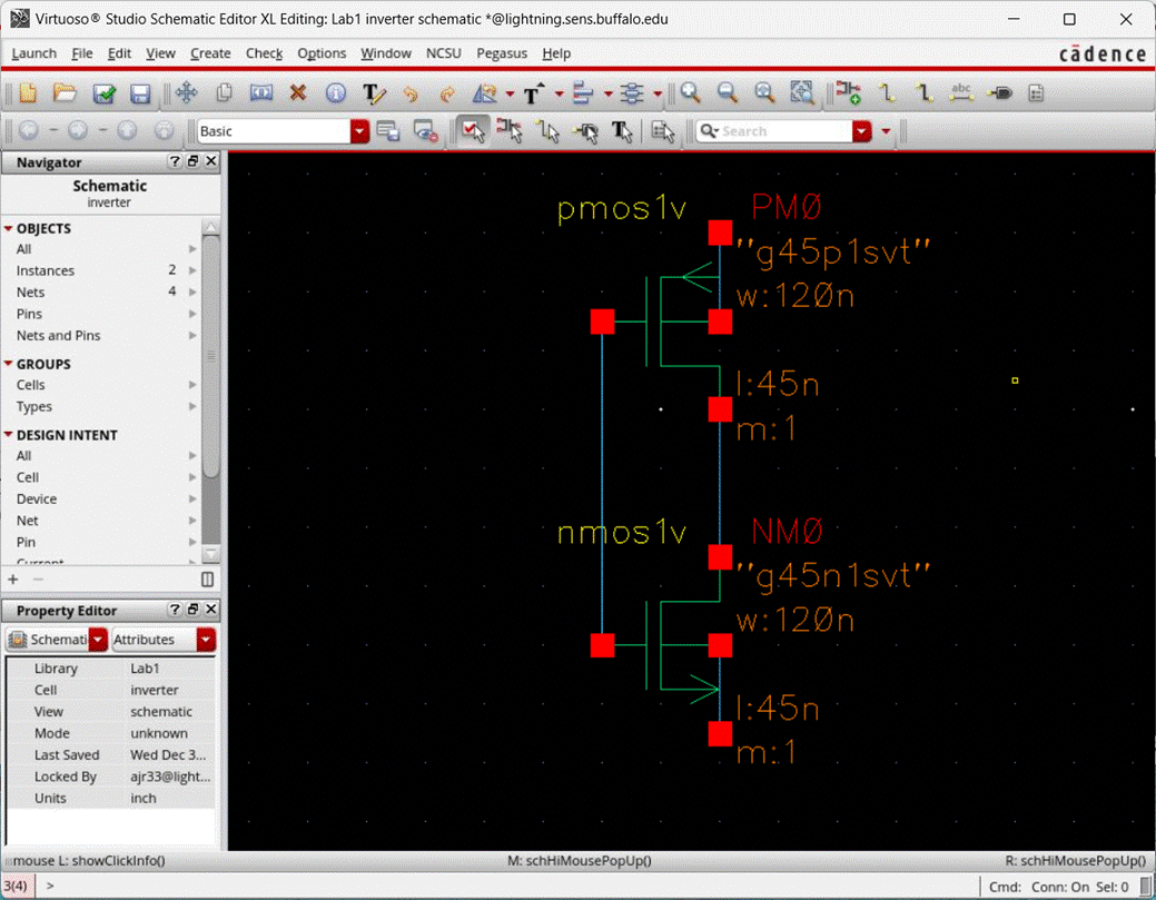
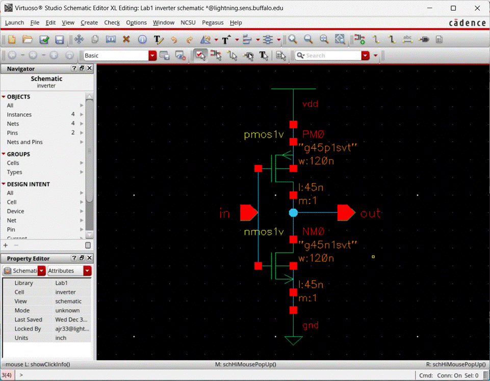
In this
case, connect the drain terminals of PMOS and NMOS, and the gate terminals of
the PMOS and NMOS. Also, be sure to connect the bulk terminals of each
transistor to its source. After all this wiring, the schematic should look similar to this :
Creating
Supply Voltage Net (vdd/gnd)
and Input/Output pins:
To connect
the source terminal of PMOS to vdd, instantiate
the vdd from the analogLib
and place on top of the PMOS in the schematic. Similarly instantiate gnd and place on bottom of the NMOS transistor.
Connect the vdd terminal with the PMOS
source terminal, and the gnd with NMOS
source terminal. Next, create pins for input and output. Click on
"Create->Pin..." (or type p) in the schematic window, the
following dialogue box would appear:
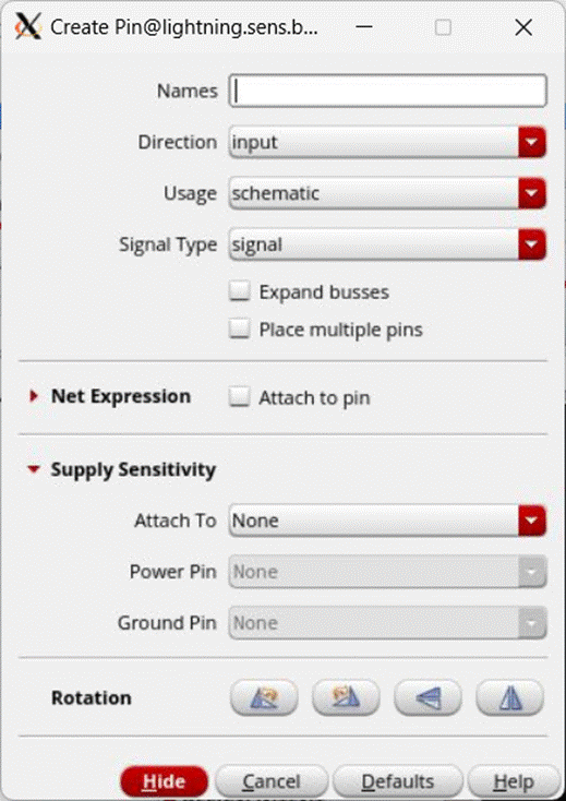
Type in as
the pin name. Note that the direction is listed as input. For an output pin,
you would need to change this to output. Press Enter, then in the schematic
window, place the pin terminal on the wire that connects the gate terminals of
the transistors. Similarly, create an out pin and set
its direction as output. The out pin is placed on the wire connecting the drain
terminals of the transistors. After this, the schematic should look similar to this:
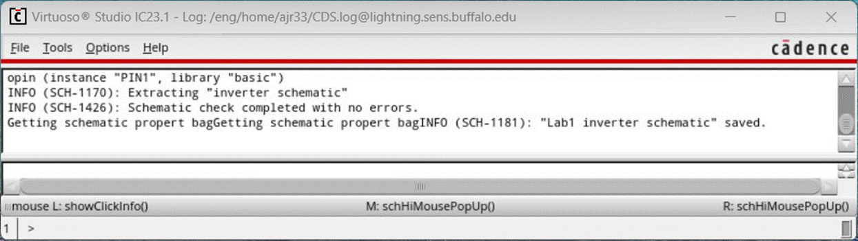
After
the design has been completed, click on File -> Check and Save to check and
save your designs, or use hotkey F8.
Check the CIW window to see if there are any errors or warnings in
your design. If there are, then fix them and repeat Check & Save.
Transient Simulation using
ADE Explorer
To
simulate the current design, in the Virtuoso window, click on Launch->ADE
Explorer. In the Launch window, choose Create New View & press
OK. If you have a saved simulation already, you can use Open Existing View to
view saved simulations.
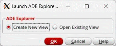
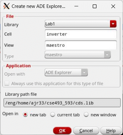
In the Create
New ADE Explorer window, make sure that the Library is
Lab1, cell is inverter & view is maestro.
You can
specify whether you want to open the view in a new tab, current tab, or new
window. Click OK to open ADE Explorer.
Once
ADE Explorer opens, the window should look like this:
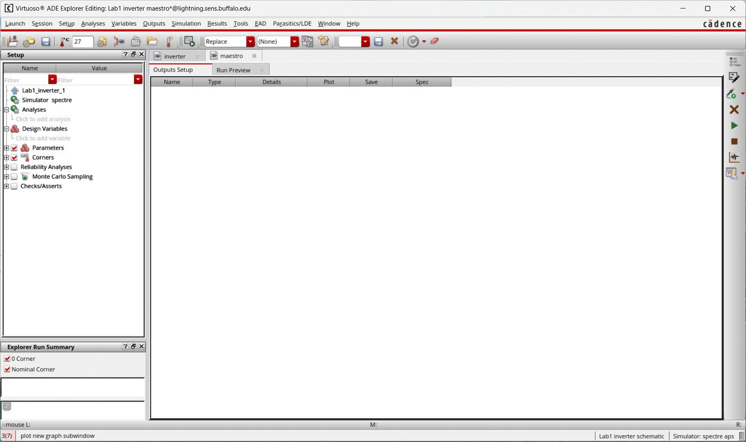
The
following points have to be taken care of before the
design can be simulate
·
Setup -> Simulator: specifies the
simulator to use. Set the simulator to spectre.
Press OK to save.
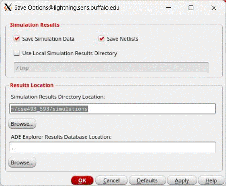
·
Setup -> Save Options: specifies what
to save & where the simulation results will be stored. The simulation
results will default to <home directory>/cse493_593/simulations location.
Press Ok to save.
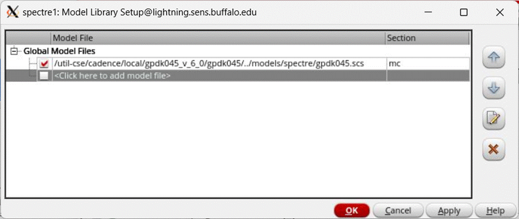
· Setup -> Model Libraries: Specifies the path for the model
files. This should be set by default, but if not set it to /util-cse/cadence/local/gpdk045_v_6_0/gpdk045/../models/spectre/gpdk045.scs
· Set the section to use mc (Monte Carlo) & press OK to save.
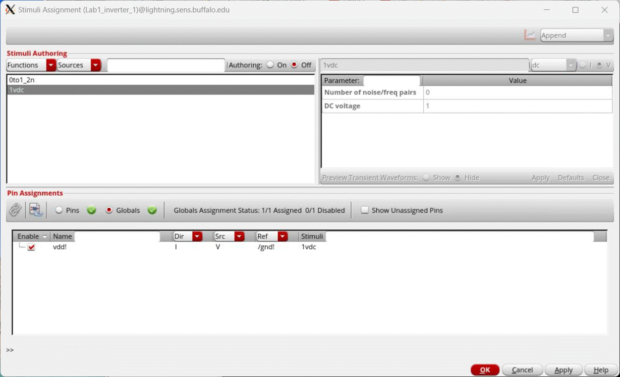
- Setup -> Stimuli: Specifies the input
parameters & voltages for the circuit. The Stimuli Assignment window
should come up & look like this.
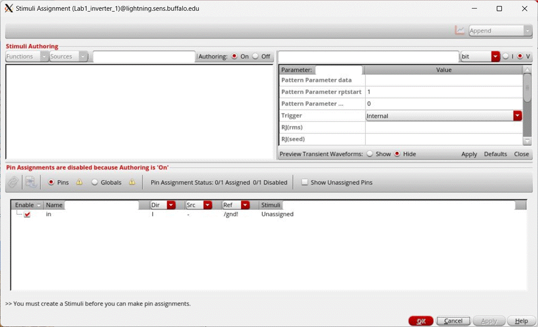
To assign stimuli to pins you
first need to author a stimuli. Do this by setting
parameter data in the upper right side of the assignment window.
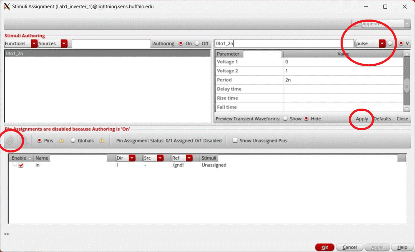
For this inverter, we will
set the input pin to go from 0V to 1V at a period of 2ns & a pulse width of
1ns.
1.
Turn Authoring On.
2.
Set the function to pulse & make sure that V (voltage source)
radio button is selected.
3.
Set the following in the parameter menu:
a.
Voltage 1 = 0
b.
Voltage 2 = 1
c.
Period = 2n
d.
Pulse Width = 1n
4.
Give a name for the stimuli & click Apply that is
underneath the parameter view.
The stimuli that you just
created should appear under the Stimuli Authoring section.
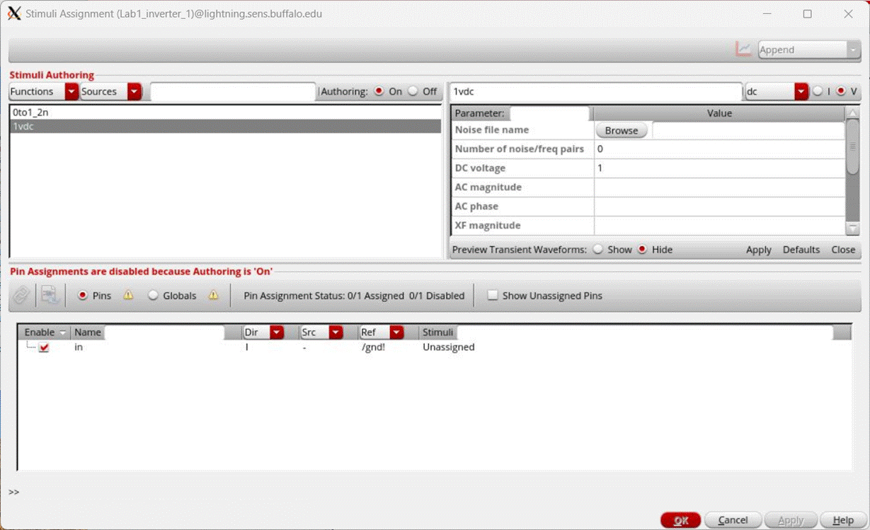
Create another stimuli for VDD. Set the following parameters:
a.
Function = dc
b.
DC voltage = 1
Once you have the two stimuli
setup, the window should look similar to below:
To
assign stimuli to pins, turn off Authoring with the Off radio
button under the Stimuli Authoring section.
In the
Pin assignments section click on Pins to view all the input pins for the
schematic.
Use the
Enable checkbox to enable the pins to set stimuli for, disable pins that are
unnecessary.
Click
the stimuli to assign to the pin & also click the pin (pins) that you want
to assign to.
Click
the chain icon underneath the Pin Assignments section to assign the stimuli.
To
unassign pin(s), right click & select Set Selected Pins to Unassigned.
Click
on the Globals radio button to view the global
sources.
Assign vdd! to the 1V DC stimuli.
Once
all enabled pin assignments have been assigned stimuli, Pins & Globals will have green check marks. Click OK to save
stimuli.
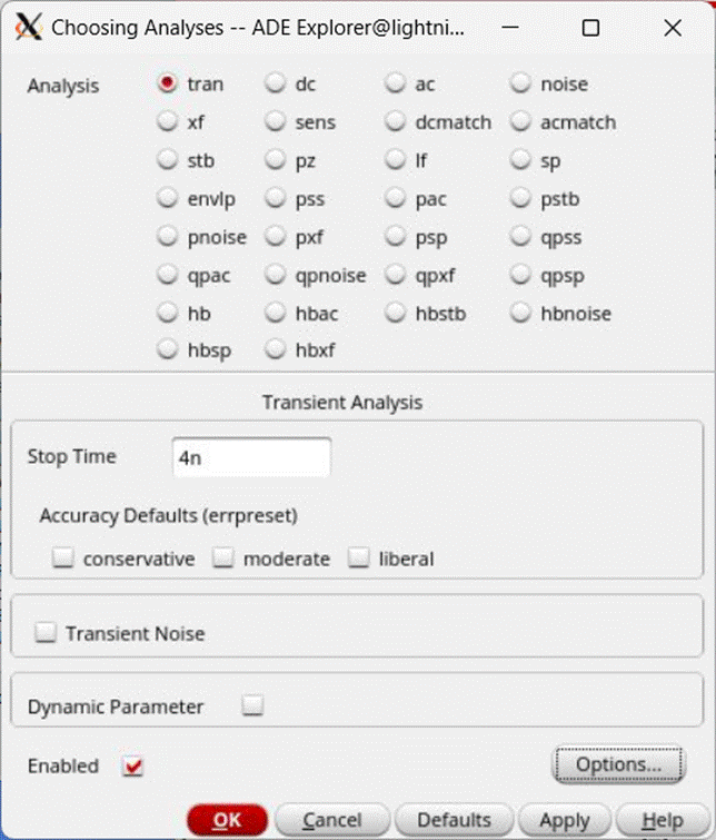
- In the next step, we choose what analysis is to
be performed. We will perform a transient analysis for 4ns and plot the
waveforms for the inverter input and output.
- Click on Analysis -> Choose. On the Choosing
Analyses window, click on tran and
enter 4n for the stop time.
- Make sure that the Enabled checkbox is
checked then press OK to save.
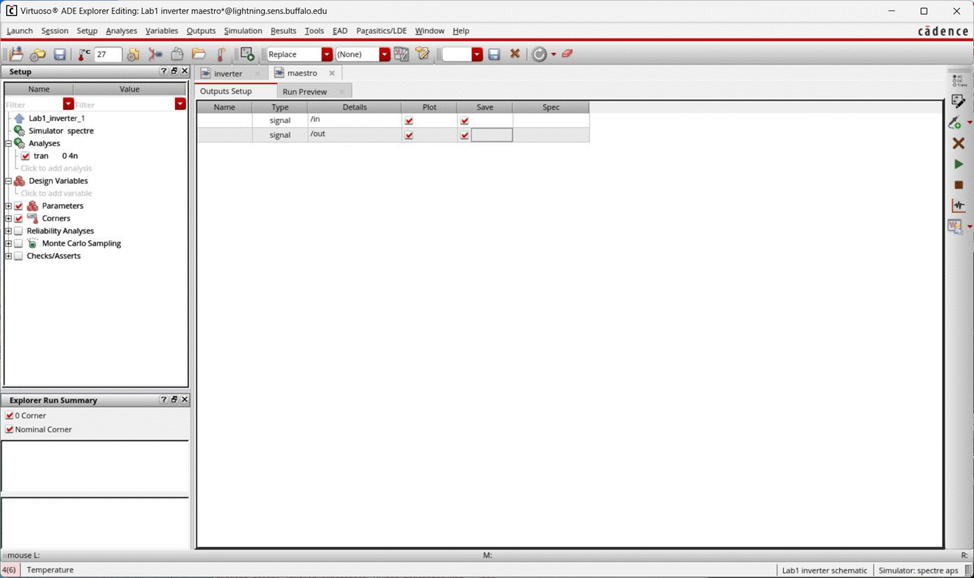
· Add the signals
to keep track of under Outputs -> Add -> Signal.
o
Also add from the probe icon on the right.
· Under
Details, enter the name of the pin to output. In this case type in.
o
You can also choose a pin from the schematic itself by clicking
the ellipses, then clicking the pin/net to track.
· Under the
save column, check the in pin to save its output.
· Create
another signal to track the output pin out.
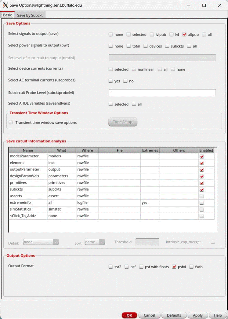
· To save the voltage waveforms in the
circuit, click on Outputs -> Save All in the ADE window. In the Save Options
dialog box, select as shown below and click OK:
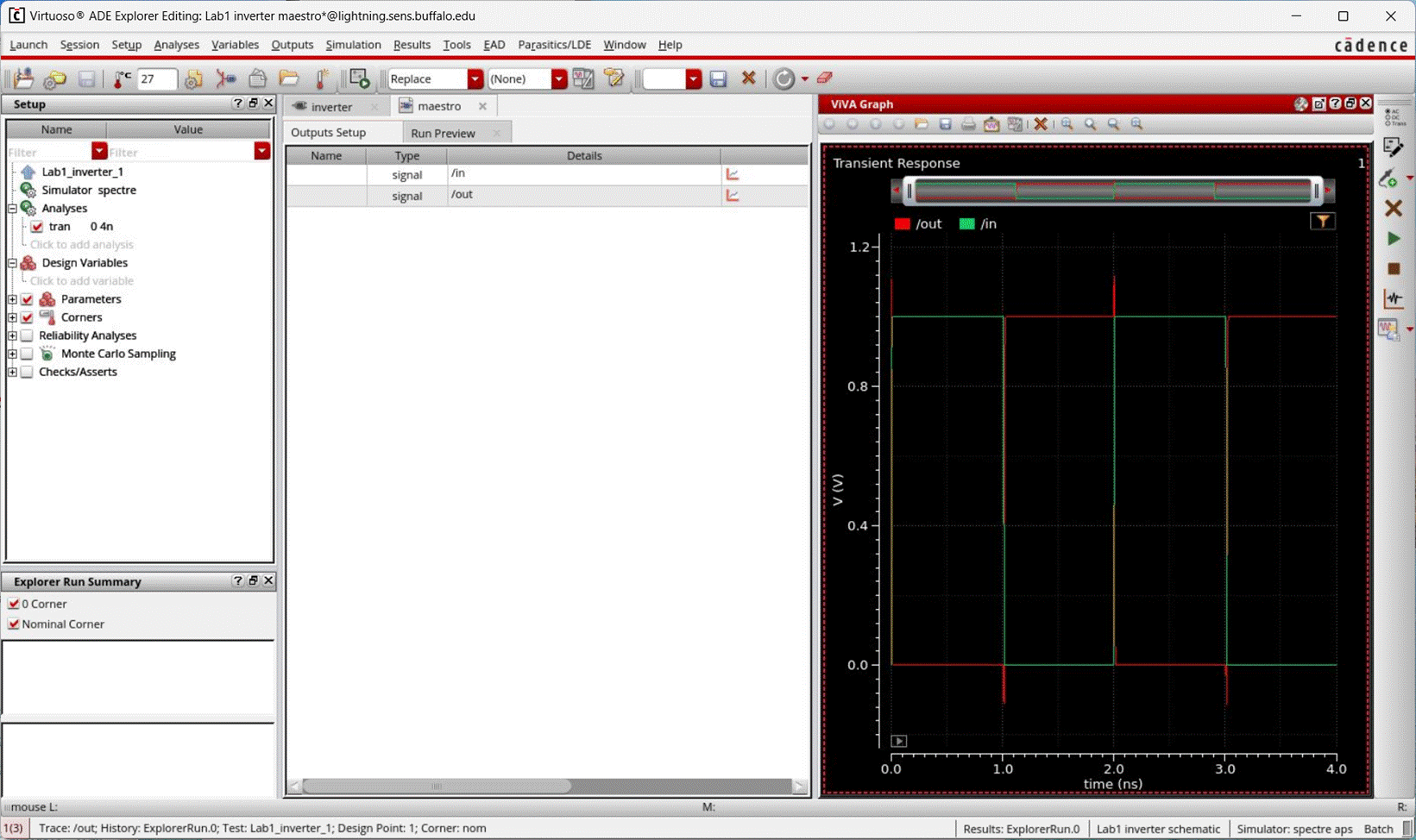
· The ADE
Explorer window should look similar to this:
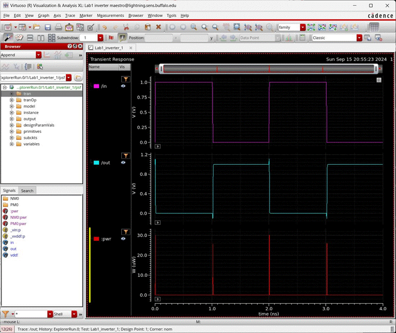
- To run the simulation, click on Simulation >
Netlist and Run. Check if there are any errors or warnings in the CIW
window and fix them. If the simulation completed successfully without 0
errors, the simulation results are ready to be viewed.
- The graph is opened automatically with the
selected signals to plot.
·
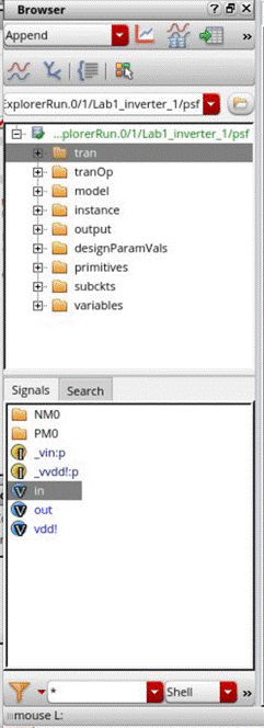
To view the graph in a separate window, click Tools
-> Results Browser.
·
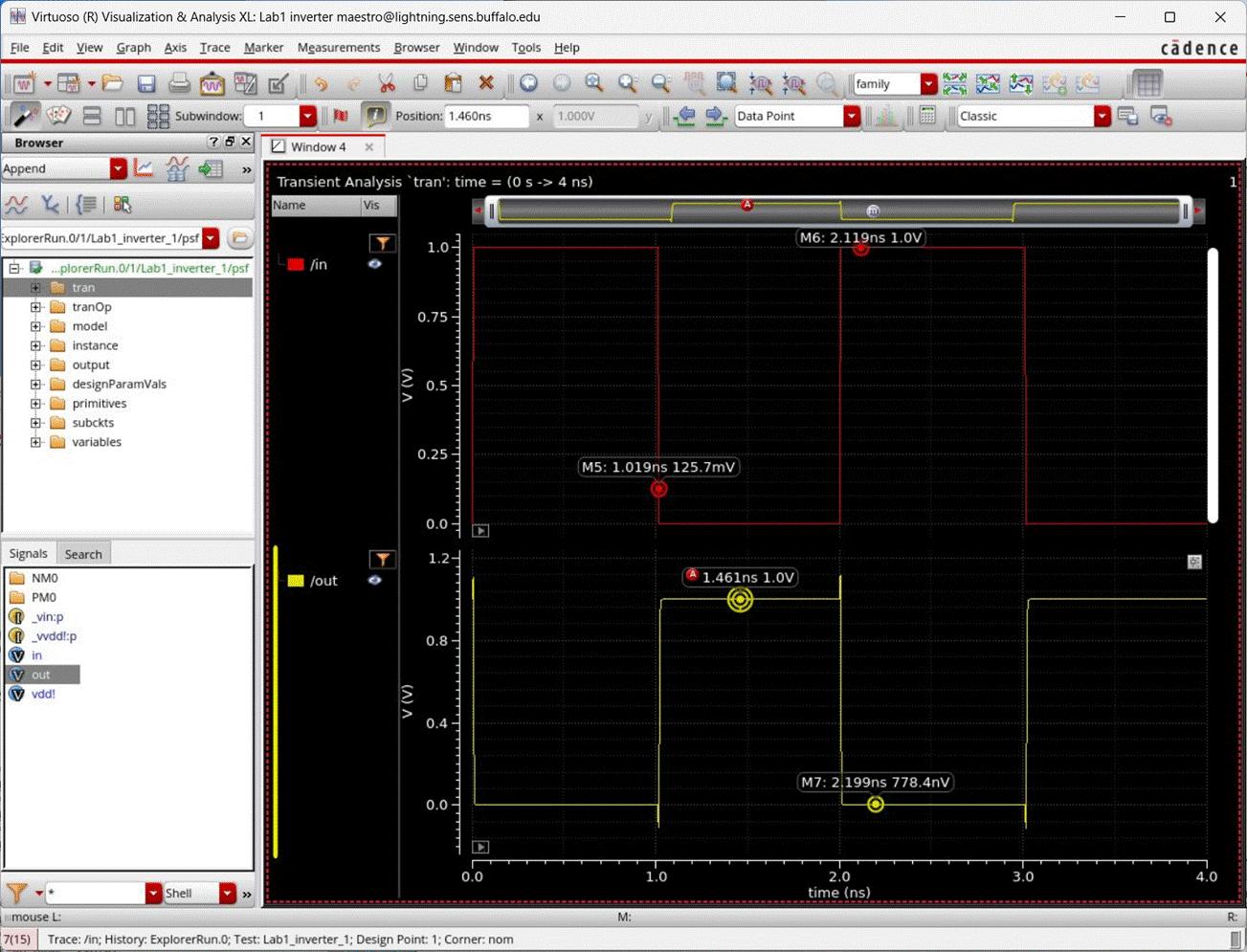
In the results browser window, click on tran in the left side pane. That yields a window like this:
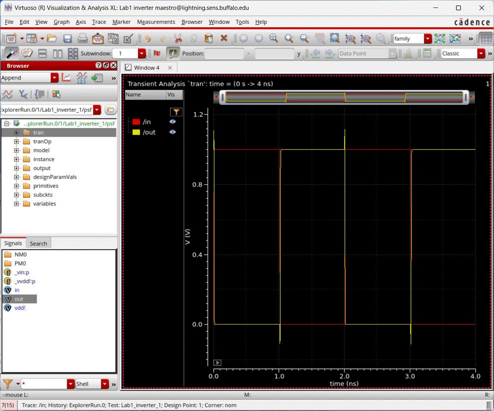
- To plot a signal that is not already on the
graph, find its name on the left hand pane and
double click it.
- After double clicking on the signals, the
Visualization & Analysis Window looks similar to
this:
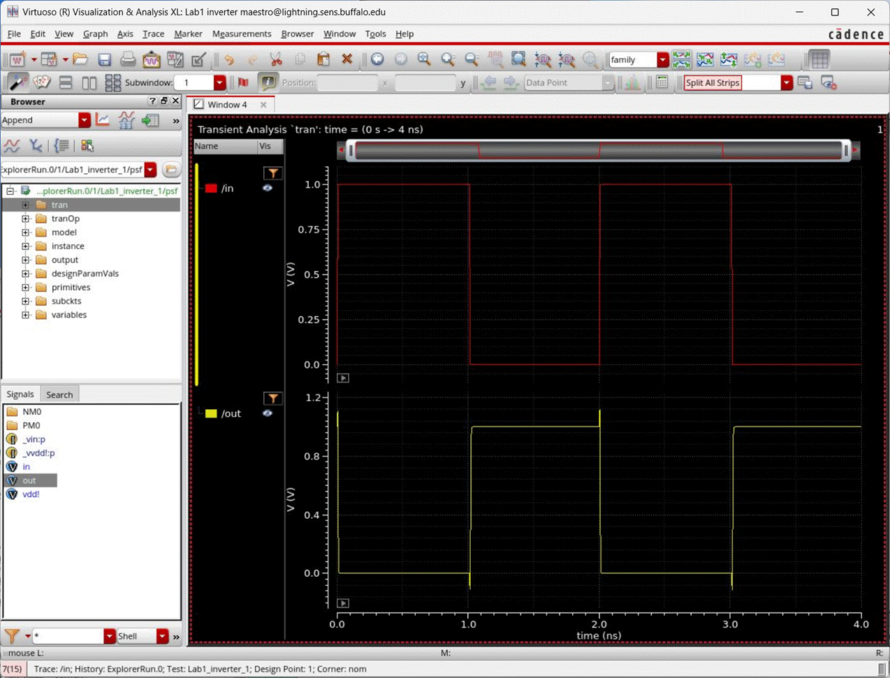
- There are several methods to analyze the waveform
in the waveform window. The hotkeys are most useful include
·
f: fits waveform in current window display
·
]: zoom in
·
[: zoom out
·
v: vertical tracker
·
Split
each signal to each of its own axis by selecting Graph -> Split All Strips.
·
Marker A: Pressing A on a graph will create a marker based on the
location of your cursor. Pressing A again will update the A marker based on
your cursor location again.
·
Marker M: Pressing M on a graph will create a marker based on the location
of your cursor that will stay until removed. M markers are labeled M1, M2, M3 etc
·
To remove a marker, click on a marker & press the delete key
or right click on a marker and select Delete.
·
Markers are a useful way in measuring
delays and rise/fall times of signals.
Quit the ADE Explorer session with the Session -> Quit option.
Import Simulation States
The simulation state can be reloaded when it is saved to another
simulation. This allows for you to import a state & change just the stimuli
to meet your needs.
To import a simulation state, go to Session -> Import and
choose the library, cell & view to import from.
If closing the ADE Explorer window closes all the other windows,
open the library manager again with the CIE by going to Tools -> Library
Manager.
Symbol Creation and Simulation
Symbols
are useful when the schematic design is done hierarchically. At a higher of
level of abstraction, we would like to use a symbol to replace the details of a
cell. Because of this, a symbol of a cell design should define all the input
pins and output pins of that cell explicitly.
Once you have completed the schematic design, you can create its symbol right
from the schematic cell.
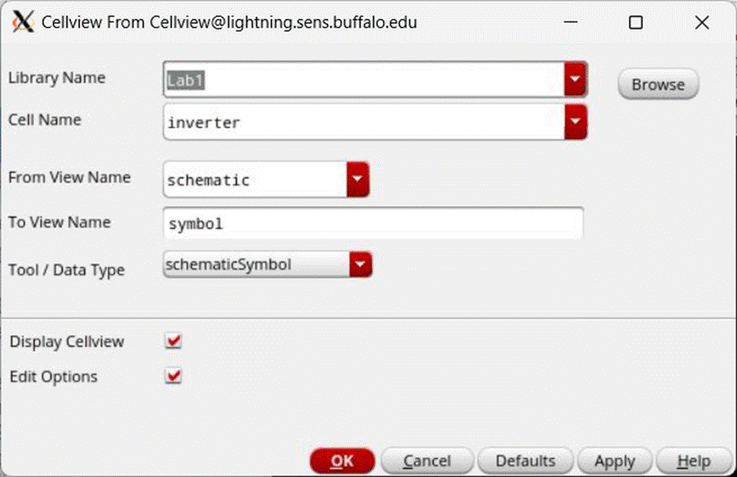
Click
on Create -> Cellview -> From Cellview. Click OK on the Cellview From Cellview window.
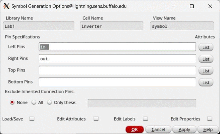
On the
next window, define the location of the pins. If you create the symbol from the
schematic cellview, the pins are auto populated as shown
below. Click OK to open the Symbol Editor.
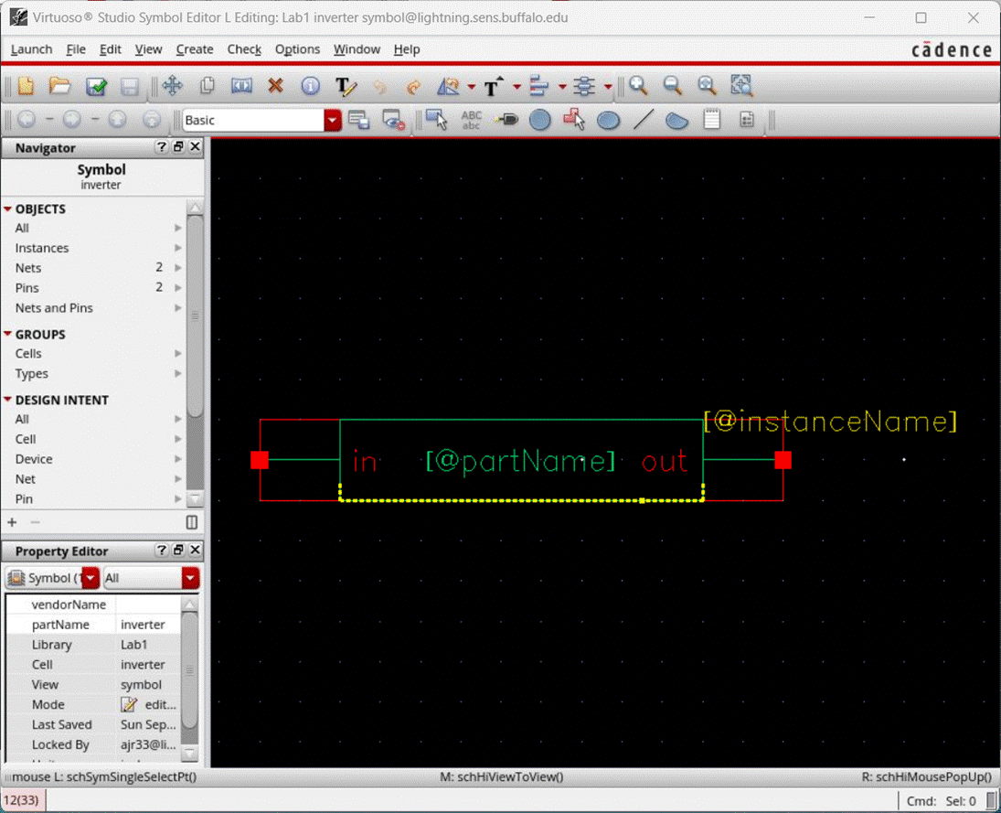
This
will pop-up another window that contains a default symbol picture, which is
shown below.
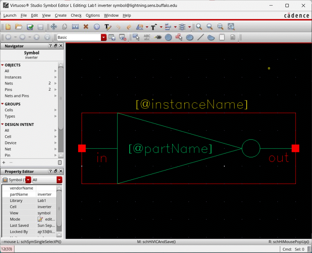
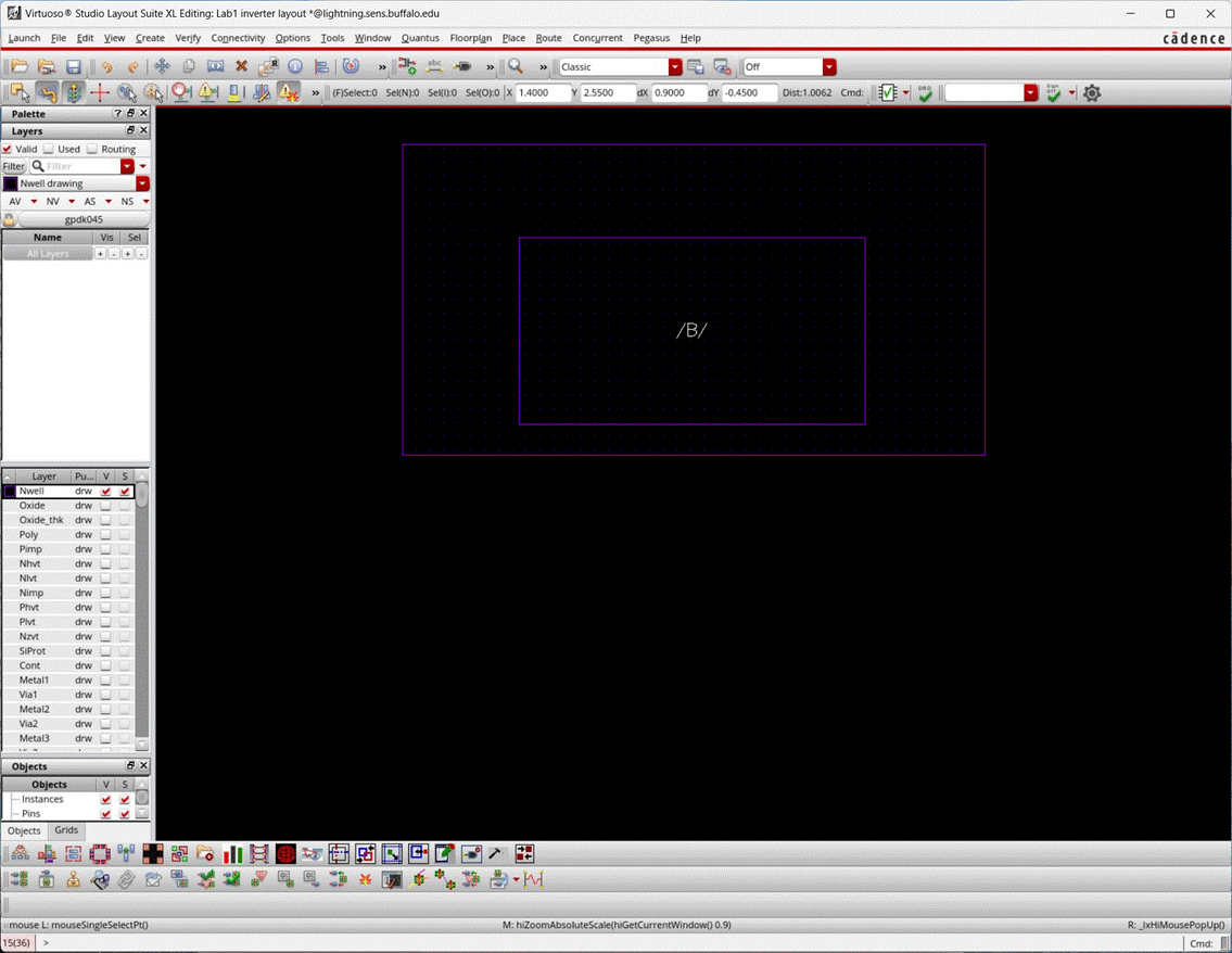
It has
a red box that encloses the green colored inverter symbol. This red box defines
the actual size a symbol will occupy, if you were to use this inverter symbol
in another design.
You can
change the size of this box by clicking and dragging. It is good custom to
exactly fit the symbol within the red box.
The red
square dots indicate the pin connections. [@InstanceName ] and
[@PartName] are display variables, which you may delete or keep.
If you don't
like this rectangular symbol that is automatically created by the tool, you can
create a symbol of you own by dragging the lines and input/output pins to their
desired locations. An example is shown below, in which an inverter symbol is
created which looks similar to the usual inverter gate symbol:
Once
the symbol is created, it can be instantiated in any other cell design. For
example, you may create a new schematic cell view (could be under the same
library Lab1) to design a ring oscillator. A ring oscillator consists of a
chain of inverters. You could instantiate the inverter symbol we just created.
To do
this - press hot key i or click on Create
-> Instance. In the component browser window, click on Lab1 -> Inverter
and place the required number of instances in the ring oscillator schematic.
After
Checking and Saving the ring oscillator schematic, it can be simulated using
the same procedure described above.
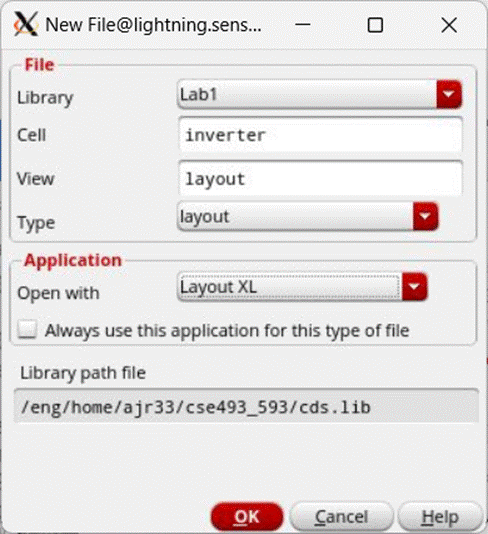
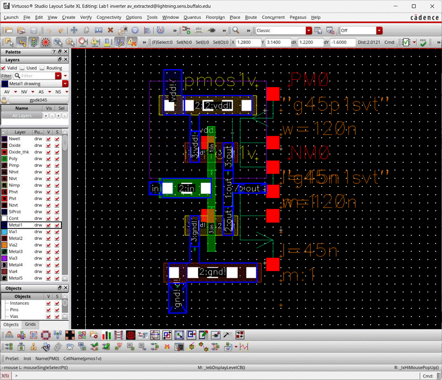
Now, we
will go through custom layout using Layout L, by creating a layout for the inverter
cell. To do this, in the Library Manager window, click on File -> New ->
Cell View.
Select
Type as layout & Open with as Layout XL. Click OK to open the layout view.
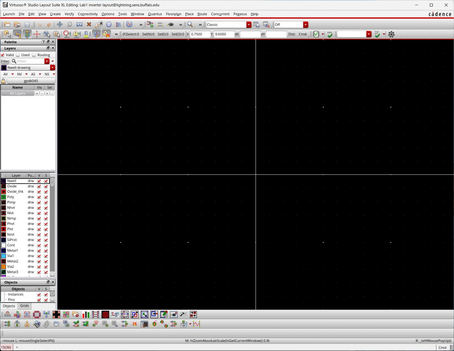
If the
license window pops up, click Session or Always. The schematic
view & the Virtuoso Layout Suite XL Editing window should open up as shown
below:
To make
grid snapping better you may want to change the snap spacing to 0.01. Go to
Options -> Display or use hotkey e to view the display options. Under X Snap
Spacing & Y Snap Spacing, set these both to 0.01 for more precise layout
positioning. NOTE: Incorrect Grid Spacing can cause DRC errors which may
have you to redo your entire design.
On the
left hand side, there is a pane that contains all the layers that would be used
to draw the layout.
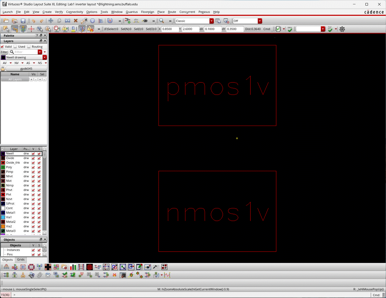
To
create the inverter layout, let us first instantiate the PMOS transistor. To do
this, press hokey i or click on Create
-> Instance. In the create instance window, enter the following:
·
Library: gpdk045
·
Cell: pmos1v
·
View: layout
·
Length: 45n
·
Finger Width: 120n
·
Total Width: 120n
·
Fingers: 1
·
S/D Metal Width: 60n
Place the
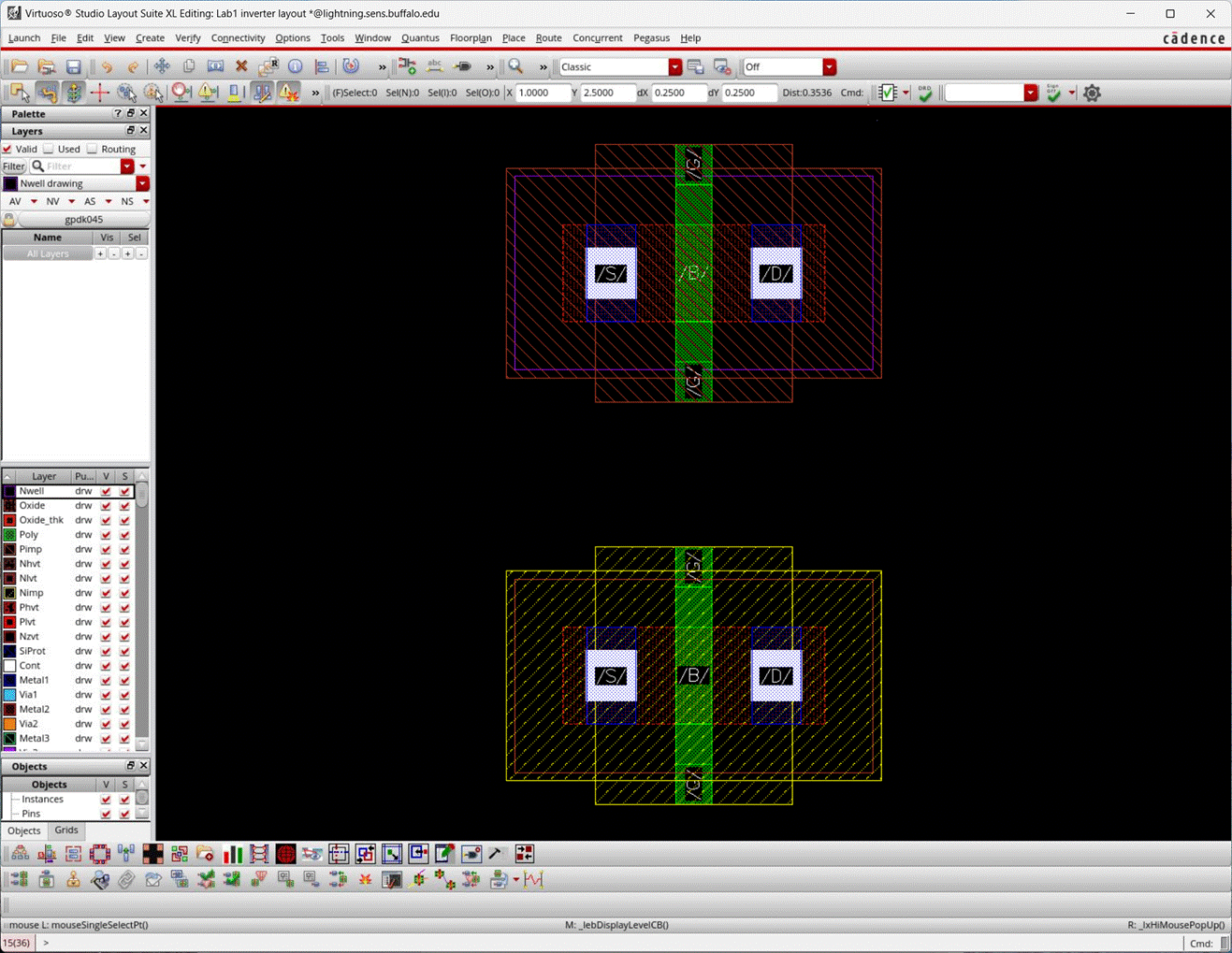
instance in the layout window. Similarly, instantiate a nmos transistor from the same library and place
below the pmos transistor in the layout
window. The layout should look similar to one shown
below.
Press ShiftF/ControlF to
toggle views.
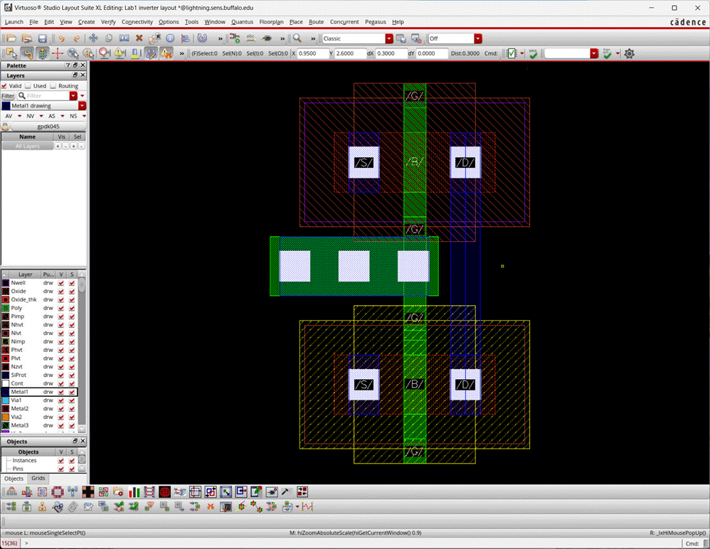
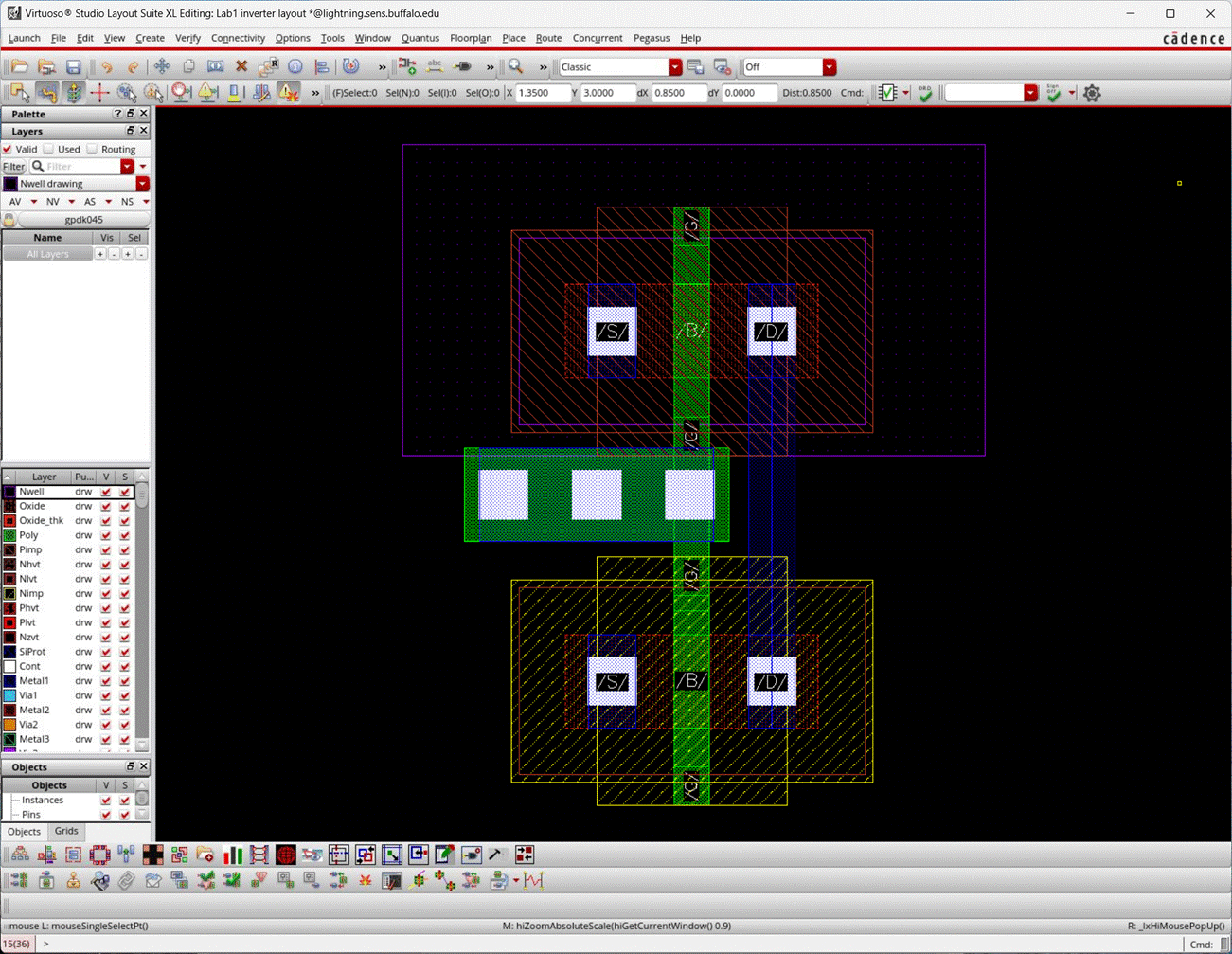
The
green rectangle (poly layer) in the middle of each transistor is the gate of
the transistor. The white filled rectangles on either side of the gate
are vias and can be used interchangeably as source/drain terminals of
the transistor. Now, we connect the gates of the pmos and nmos transistors using poly layer.
·
Left click on the poly layer in the layers pane.
·
Then switch back to the layout window and press rectangle
hotkey r. The rectangle window appears. Check the box to enable
smart snapping.
·
Switch back to the layout window, and left
click at the left bottom corner of the rectangle you want to draw.
·
Then left click at the top right corner of the rectangle you want
to draw.
Most
hotkeys used in the schematic editor work in the layout editor too. After
drawing a rectangle you might want to take a few
minutes to familiarize yourself with manipulating the rectangle shape and size.
Try using
different hotkeys such as
·
m: move
·
s: stretch
·
p: path
·
o: via
·
ctrl/shift z: zoom in/out
·
f: Fit to Window
·
k: ruler
·
u: undo
·
shift u: redo
To cancel
the current command, press ESC. At the end of this, the gates should be
connected, as shown below:
As we can
see, the width of the poly rectangle is not perfectly aligned with the gate of
the two transistors.
To fix
that select the drawn poly & press the hotkey Q. Change the rectangles Width
to 0.045 & press Apply to see the changes. Once, youre
happy with the changes, press OK to close the properties window.
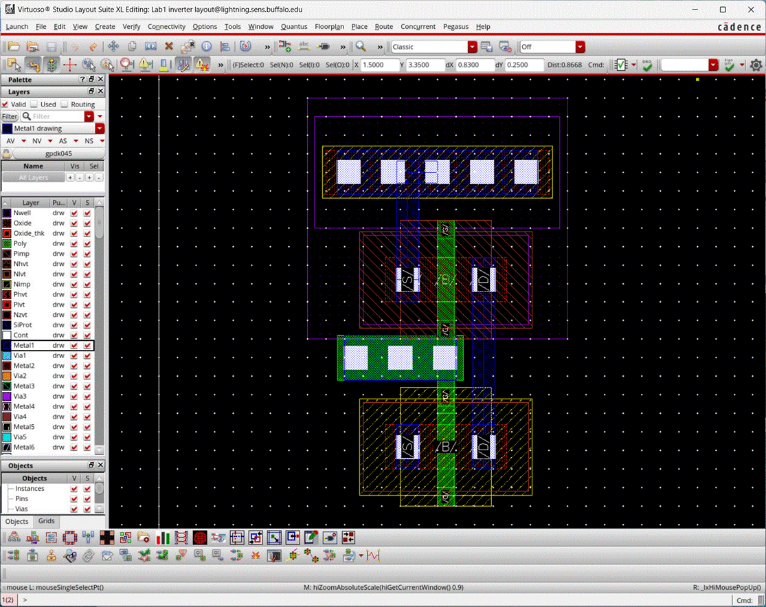
Create
a metal 1 wire (using rectangle or path) to connect the drains of the two
transistors (connect the two vias, as shown below). Use more rectangles to
draw out the wires.
The
poly layer currently is connected to our gates. We want the in pin
to connect to the poly layer. Instead of directly connecting to the poly layer,
lets use a metal as it will be more conductive than
poly.
To
transfer between two layers or more layers, use a via.
GO to Create -> Via or use hotkey o.
Set the
following parameters for a single metal 1 to poly via.
·
Mode: Single
·
Via Definition: M1_PO (Metal 1 to Poly)
·
Rows: 1
·
Columns: 3
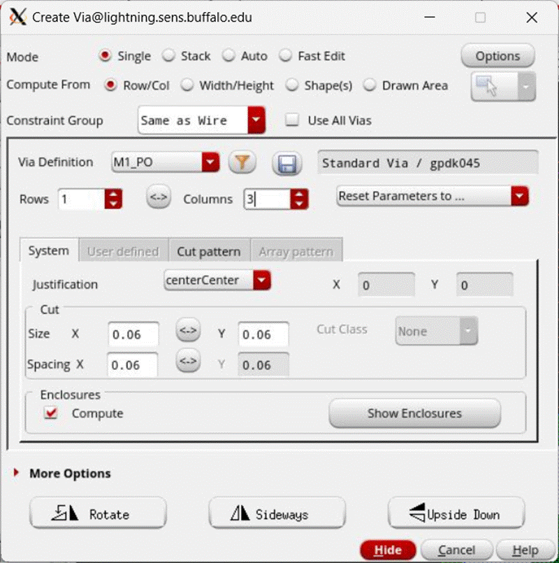
Place
the via so that the right most via is on top of the drawn poly layer to make a
connection as shown below.
Save
the layout with File -> Save.
Running DRC
DRC
stands for Design Rule Check & it make sures that the layout is following
the rules of the constraints from the foundry. In other words, a passing DRC
means that there are 0 errors & that the design is up to code for the
foundry.
It is
best practice to run DRC checks often rather than at the end of finishing the
layout so that you can catch errors early instead of later where you possibly
may have to change your entire layout.
To run
a DRC, go to Pegasus -> Run DRC
The
form should be auto populated with some defaults. Make sure that the following
are set & if not set them yourself.
·
Run Data
·
Run Directory: rundir/drc
·
Rules
·
Techonology
·
Technology mapping file: /util-cse/cadence/local/gpdk045/pvtech.lib
·
Technology: gpdk045_pvs
·
Rule Set: 493-593
·
Input
·
Library: Lab1
·
Cell: inverter
·
View: layout
·
Convert Pin to: Geometry + Text
·
Run RV checked
When choosing the Library,
Cell, View you can press this icon:
to populate the form with the
data of the current active window.
Click on Submit to run the
DRC. Save resources if prompted.
The Pegasus Results Viewer
should automatically open when DRC has completed.
In the
Pegasus Results Viewer, you can see a number of errors
that pertain to the layout currently.
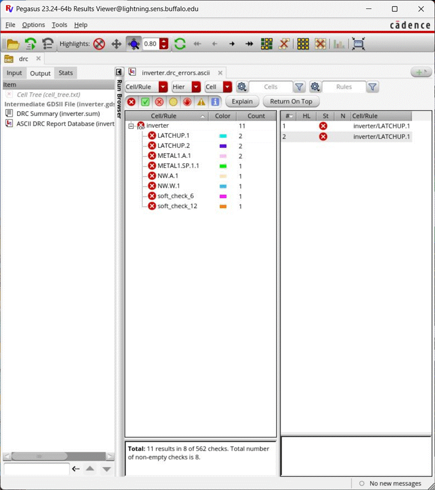
Double
clicking on a rule error will zoom into the error on the layout. This is very
useful for debugging where errors are & fixing them.
Close
the DRC Result Viewer & the report viewer by clicking on the Close Report
button in the Pegasus Reports window. We will fix these errors as we continue.
You can reopen the report very easily by going to Pegasus -> Recent Runs
-> drc.
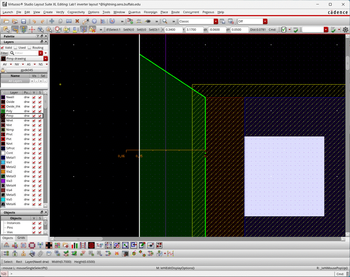
Were going to take the NW.A & NW.W errors first. They are nwell errors that specify that the minimum nwell area is >= 0.18m & that the minimum nwell width is >= 0.3m.
Back in
the layout we can see that Nwell is used for the pmos transistor. Take a rectangle & draw over the nwell so that it includes the entire pmos
transistor within it as shown below.
Filter
the layers by selecting the layer you want to see &
selecting NV at the top of the layers pane. Show all layers again by
clicking the AV button.
Filter
the nwell layers by clicking on the nwell layer then select NV. You should see both rectangles
only on the view as shown below.
Verify
that your layout is similar to above & click AV to
show all the layers again.
Run DRC
again to verify that the nwell rule errors do not
appear anymore.
Create
another via from M1 to NWELL that have 5 columns and 1 row. Place the via above
the pmos transistor.
This
via is going to be used for connecting vdd! to the nwell. We use 5 columns of vias to ensure better contact
although 1 column would work.
Connect
the metal 1 source of pmos to the via to create a
path for vdd to connect through.
To
tightly fit the layout, deselect any components then use the Stretch tool with
Edit -> Stretch or by pressing hotkey s.
Going
into the stretch tool with a component selected will move the entire component.
Without any component selected, you can freely selected
an edge of any component to stretch or shrink to your desired fit.
By now,
your layout should look similar to this:
Run DRC
again. If your DRC shows NW.E rule error, youll need
to increase the distance of the oxide layer and the nwell
layers.
To
create a ruler measurement, go to Tools -> Create Measurement or use the
hotkey k. Clear measurements with Tools -> Clear All Measurements or use
hotkey shift k.
Start
at the edge of the oxide layer & measure up to the DRC specification
(0.06m).
Now you
can easily stretch the nwell edge in
order to pass DRC.
Add a
via from metal 1 to p-substrate (M1_PSUB) with 5 columns, underneath the nmos transistor.
Connect
the source metal 1 of the nmos to the via to create a
contact for ground (gnd!) to flow through.
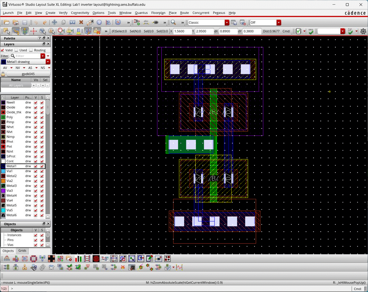
Your
layout should look similar to this once all DRC checks
pass:
Running LVS
LVS
stands for Layout vs. Schematic. It is a check that compares a layout with a
schematic & sees if all the nets, inputs & outputs match. An LVS
passing means that your layout in ideal circumstances, would perform exactly as
your schematic did in simulation.
To run
LVS, go to Pegasus -> Run LVS
The
form should be auto populated with some default values
but you MUST make sure that the following are set to run LVS correctly:
·
Run Data
·
Run Directory: rundir/lvs
·
Rules
·
Technology
·
Technology mapping file: /util-cse/cadence/local/gpdk045/pvtech.lib
·
Technology: gpdk045_pvs
·
Rule Set: 493-593
·
Input
·
Layout
·
Library: Lab1
·
Cell: inverter
·
View: layout
·
Convert Pin to: Geometry+Text
·
Schematic
·
Library: Lab1
·
Cell: inverter
·
View: schematic
·
Output
·
Additional Output
·
Create Quantus Input Data checked
·
Data Dir: svdb
·
Run RV checked
Once you have verified these
settings are set, click on Submit button to start the LVS job.
You should see the following
window when the LVS job completes:
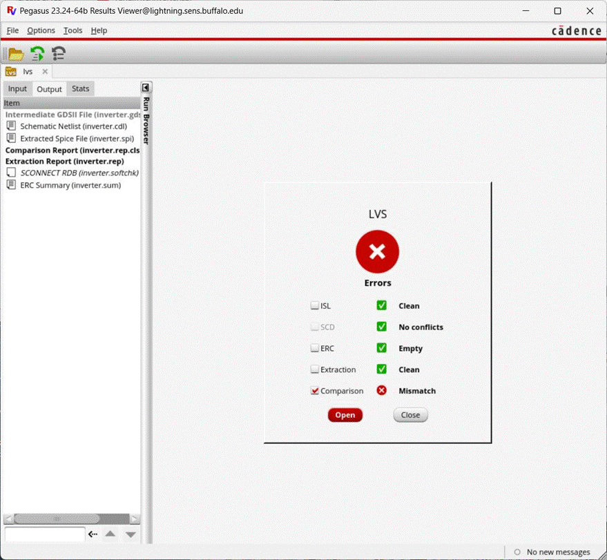
LVS did not match the
netlists so click on Open to view the report.
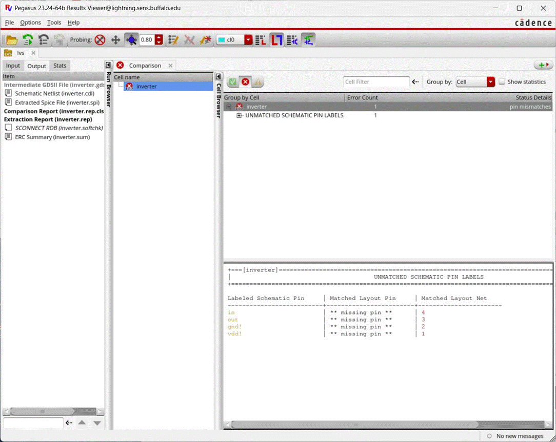
From the report, click on
inverter on the right pane to view the cell specific errors.
We can see from the report
that each of the four pins from the schematic were unable to be matched on the
layout.
Next, will fix the errors so
that LVS passes.
Close the report with the
Close Report button similar to DRC.
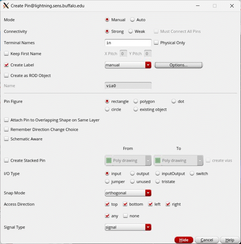
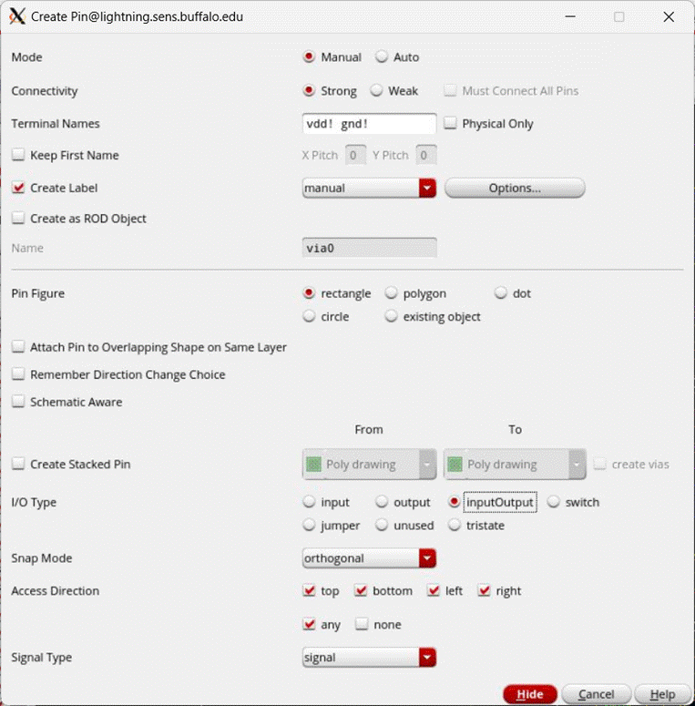
To create a pin on the layout go to Create -> Pin.
In the following window, set
the following:
·
in as the
terminal name
·
Check the Create Label option
·
Click on options & check auto under Height. Click OK.
·
You can also set the height as you like (0.1) is pretty good for
these small devices.
·
Select input for I/O Type
Select the metal 1 layer to
create the pin on metal 1. Metal is always a good choice for pins as it is the
most conductive.
Place
the pin on top of the M1_POLY via that connects the two gates of the
transistors. Placing the pin is similar to placing a
rectangle. Clicking once will start the pin at that corner. Clicking again will
create the whole pin. Next, click where you want the pin label to appear.
Ideally, pick a spot that only has one layer underneath the pin so that later on there is less confusion as to what the label
connects to.
Similarly,
create a pin for the out pin. This time, set the I/O Type as
output. Place this pin on the metal 1 between the two drains of the
transistors.
Lastly,
create the vdd! & gnd! pins. For pins that have the same properties,
you can specify multiple terminal names (separated by spaces) & the tool
will allow you to place more pins until the terminal names list is done. Set vdd! & gnd!
pins to inputOutput I/O Types.
Therefore,
you can specify vdd! & gnd! in the terminal names list as shown below:
If the
labels of pins are too big you can edit them by clicking the label &
selecting Edit -> Basic -> Properties or using the hotkey q, and change the height of the label from there.
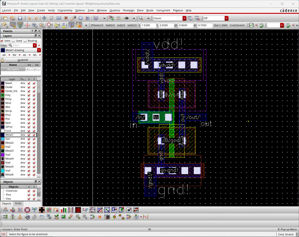
Once the
pins are created, your layout should look similar to
this:
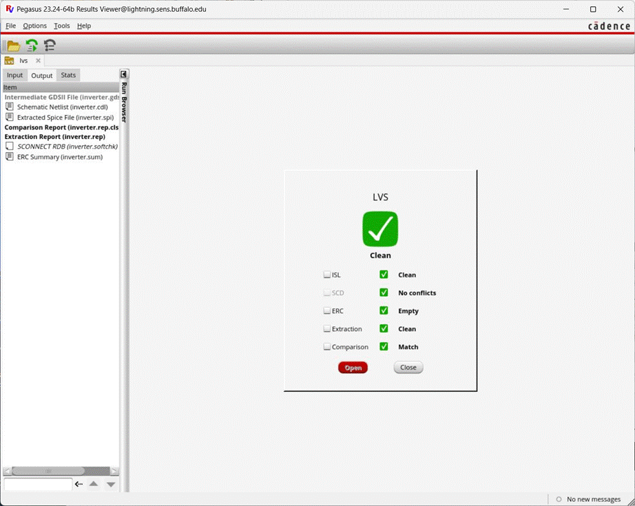
Run LVS
again under Pegasus -> Run LVS & make sure that the form options are
correct.
LVS
netlist should now match with the following window.
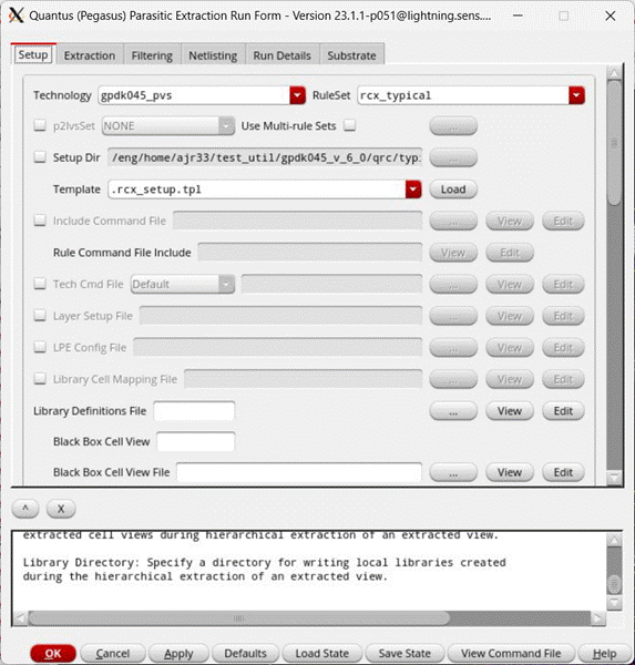
Parasitic Extraction with Quantus
Once
DRC & LVS checks pass, the next step is to do a parasitic extraction of the
electrical circuit netlist from the layout.
To set
up the parasitic extraction, click on Quantus ->
Run Pegasus Quantus. The interface window should pop
up and be already prefilled from the latest LVS ran as shown below:
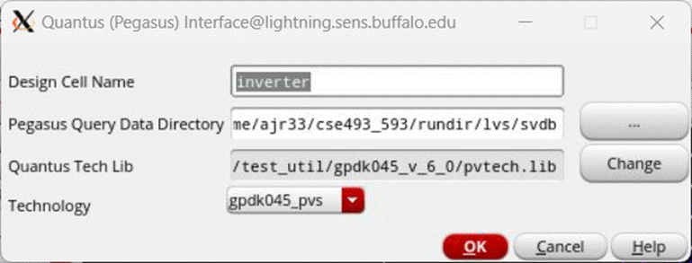
Notice
that the svdb file as the directory from the LVS
Output options earlier. Quantus can only be ran after
an LVS of the layout has been ran so keep this is mind.
Click
OK and set the following:
·
Setup
·
Technology: gpdk045_pvs
·
Rule Set: rcx_typical
·
Output: Extracted View
·
Lib: Lab1
·
Cell: inverter
·
View: av_extracted (you can pick a name
if running multiple extracted views)
·
Extraction
·
Extraction Type: RC
·
Cap Coupling Mode: Decoupled
·
Ref Node: gnd!
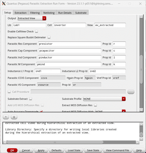
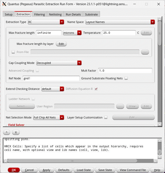
After the forms parameters are set,
click OK to start the extraction. This will take a few seconds.
Once done you should see a popup
saying that the extraction completed & its location:
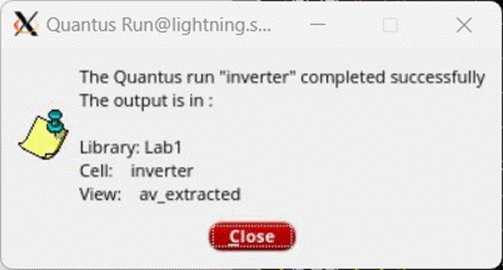
If there are errors, view the
error report or check the CIW for more information.
Once
the Quantus run is complete, go to the Library
Manager window and open the extracted cell view for the inverter. It should
look similar to the window shown below. If it doesnt try toggling the view with Shift F/Ctrl F.
Now the
extracted layout is ready to be simulated. To simulate it, follow the same
steps as specified in the Simulation section
above.
Similar
to
creating symbols at the schematic level, your layouts can also be instantiated
and repeatedly used several times while designing a hierarchical design. Let us
go back to the inverter example. Create a new layout cell view for the inverter cell.
Create an instance by clicking Create > Instance in the layout window. Then
browse to the Lab1 library, inverter cell and select the layout. This
can now be instantiated in your layout multiple times and used similar to the schematic symbols. The layout can be DRC
verified, extracted and simulated using the steps
described above.
Waveform
calculator can be used to perform may different measurements/transformations on
the waveforms displayed in the waveform window. This includes computing the
average of a waveform (e.g. power) over the entire length of the simulation or
in a given period of time, finding the propagation delay of between input and
output signals, or addition/subtraction/multiplication/division of waveforms,
etc.
Example:
Let us compute the average power consumed in a circuit during time 0 to 2ns. To
do this, make sure that before simulation you select the Outputs > Save All
> power (all) option in the ADE Explorer window. Then simulate the circuit
as usual, with simulation time more than 2ns.
In the
waveform graph window, click on Window -> Assistants -> Browser to open
the Results Browser. Click on the psf file + icon to
drop down & click on the tran folder to see all
the signals from the transient output. :pwr is the
instantaneous power consumed by the whole circuit. Double click to view the
power waveform.
To
invoke the calculator tool, click on Tools -> Calculator.
The
calculator window shown below appears. Make sure Wave and Clip are selected.
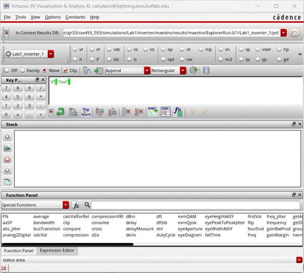
Now
switch back to the waveform window and left click the mouse once on the power
waveform. Then switch back to the calculator window. It should look as shown
below. The name of the waveform that you clicked on has appeared in the white
box in the calculator.
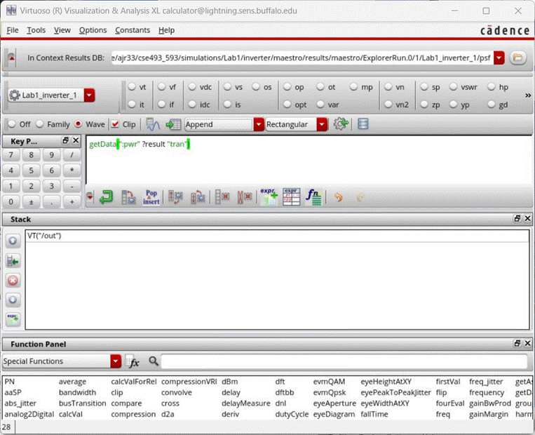
Next,
we will choose the operation to be performed on the waveform. To get the average
power between 0 and 2ns, we first clip the waveform to the time interval of
interest. To do this, click on the clip function in the list of
functions towards the bottom of the calculator. That should result in a window similar to this:
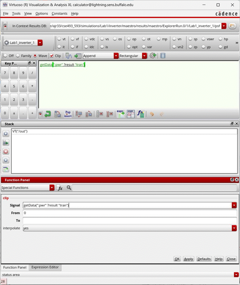
Enter
From = 0 and To = 2n in the fields. Then click on
apply. Notice that the white box above is updated now with the clip function
applied. Now this expression needs to be evaluated/plotted. To do so, click on
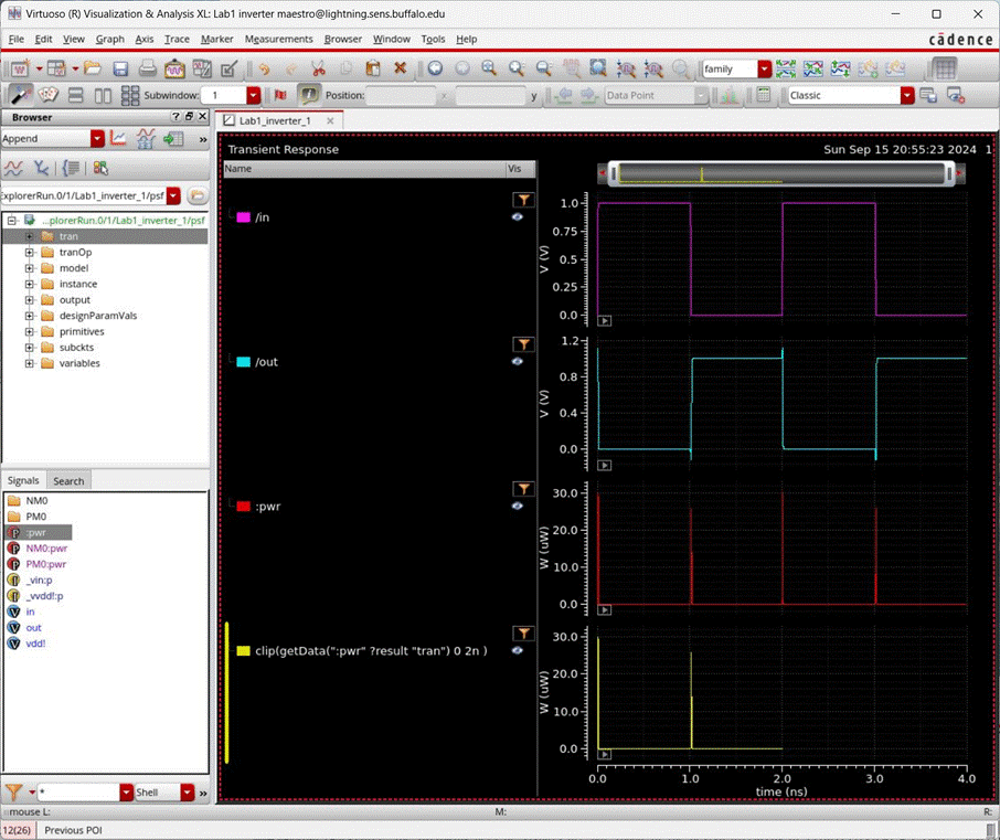
Tools > Plot in the calculator window. Switch back to the waveform window.
Now there is the clipped waveform, similar to this:
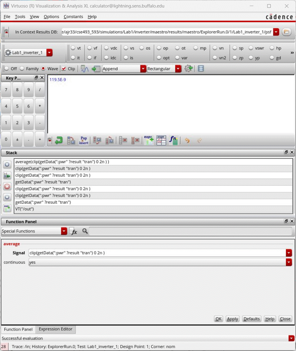
We now
need to compute the average of this waveform. Switch back to the calculator
window. If the clip function is still active in the bottom of the calculator,
click on close. The white box in the calculator should now read
something like:
clip(getData(:pwr ?result tran) 0 2n )
Select the
average function from the list of functions in the calculator then click Apply.
Then
click on Tools > Plot. This will print the average value in the white box in
the calculator.
To
select a different waveform and work on it in the calculator, simply go to the
waveform window and click on the waveform of interest. The white box in the
calculator will now be updated to that wave form.
Acknowledgement: Some parts
of this tutorial have been borrowed from the Cadence Tutorial website at
the
This tutorial has been updated
September 2024 by Anthony Roberts. Much of the tutorial was based on Aaron Carman’s Youtube
video on new GPDK045 provided by Cadence link here.