CSE
493/593 Fall 2024
Pad Frame
Introduction:
Your final project should
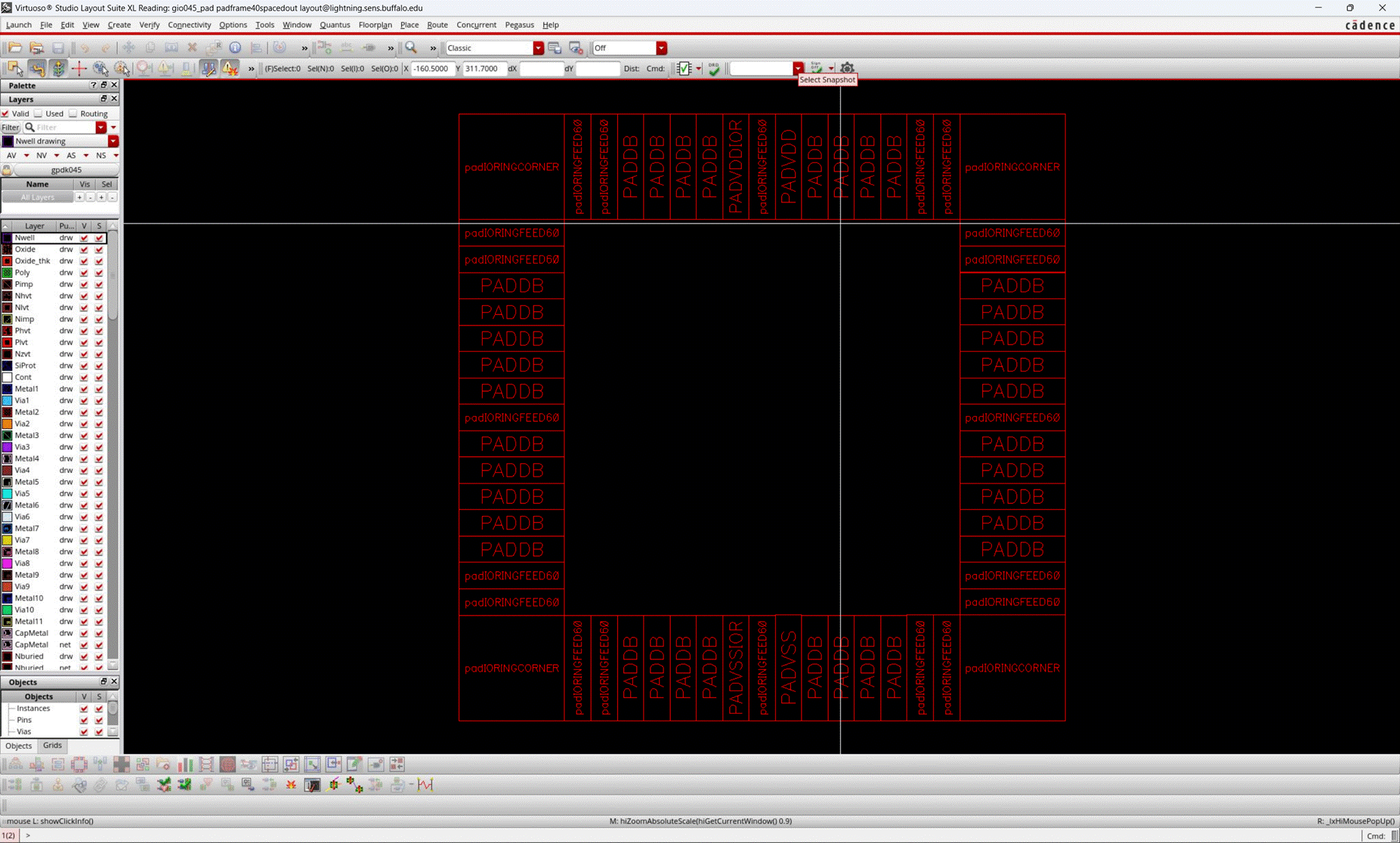
be laid out within a chip pad frame. There are a total of 40 pads in the pad
frame to supply VDD, GND, input & bidirectional input/output pins.
The dimensions around the
chip are 1300µm x 1300 µm with the inside of the chip 900µm x 900µm. Make
sure that your circuit can fit inside the area. You may need to adjust your
layouts to accomplish this.
There are 7 different types
of pads included in the schematic & layout.
|
Name |
Description |
|
CORNER |
Pad Frame corner: non-usable |
|
PCORNER |
Spacer pad: non-usable |
|
PADVDD |
VDD power pad: 1 pad |
|
PADVDDIOR |
VDD power pad for pad frame: 1 pad |
|
PADVSS |
Pad ground: 1 pad |
|
PADVSSIOR |
Pad ground ring for pad frame: 1 pad |
|
PADDB |
Pad for both buffered input &
bidirectional input/output: 36 pads |
Integrating your final
project layout with pad frame:
An example circuit name inverter2padframe40spacedout
is available for your reference in the gio045_pad library.
1.
In the Library Editor window, click on
Edit -> Library Path…
2.
Include the gio045_pad library with the
following:
Name: gio045_pad
Path: /util/cadence/CSE493_593/gio045_pad
Name: giolib045
Path: /util/cadence/CSE493_593/giolib045
3.
Save the path with CTRL-S or go to File
-> Save & close the path editor
You should now see the new libraries in your Library Manager.
4.
Create a new layout cell view in your
projects library called teamX (where X is your team letter)
5.
Instantiate the layout of the cell padframe40spacedout
from the gio045_pad library in the teamX cell
6.
Add your project layout components.
Connecting
your circuit to pad frame:
An example circuit name inverter2padframe40spacedout
is available for your reference in the gio045_pad library.
A schematic of the pad
frame is available under the cell: padframe You may use the schematic to initially
test your circuit under ideal conditions.
The layout is under padframe40spacedout.
You’re expected to have the extracted view simulations at the
project deadline.
There
are 3 pins that come out of the PADDB pad: A, Y & OE. Each pin is metal 2.
A
is the bidirectional input/output. It is suggested to use A for outputs only.
Y
is a buffered input.
OE
is the output enable pin which is active low.
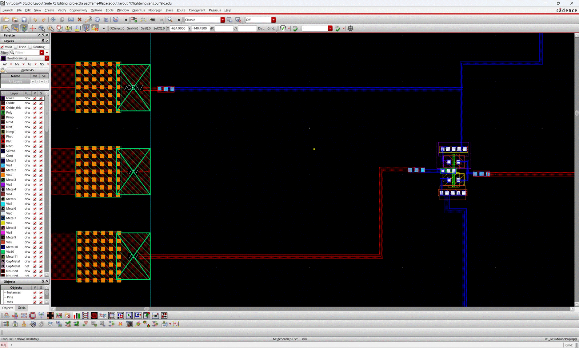
Input
signal
1. To connect an input signal, connect your component to the metal 2 Y
pin of one of the PADDB pads. Use a via if your component does not take in
metal 2.
2. Connect the OE pin to VDD.
Output signal
1. To connect an output signal, connect your component to the metal 2 A
pin of one of the PADDB pads. Use vias to connect your components through the
metal 2 layer if necessary.
2. Connect the OE pin to ground (or optionally make it a pin to trigger it
based on another signal if your circuit requires it).
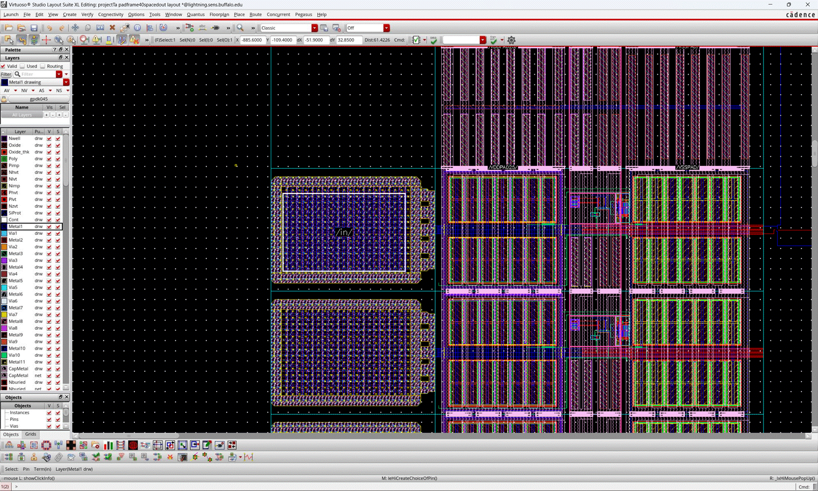
Power signals
Power signals are connected with metal 1.
1. Connect vdd! to the VDD & VDDIOR pads at the top of
the pad frame. VDDIOR is an input/output ring which supplies VDD throughout all
the pads of the pad frame.
2. Connect gnd! to the VSS & VSSIOR pads at the bottom
of the pad frame.
Pad connection
1. To connect your inputs/outputs/power signals to the pad frame, create
pins in your layout on metal 1 layer and place them on the pad.
This connects the pin to the input/output of the
components inside the chip. All pins should be outside of the chip.
Simulation with Pad Frame:
Once layout is complete, run an LVS with
output option “Create Quantus Input Data” checked & Data Dir set to
svdb
LVS is likely to failed but as long as
errors are with PADDB then it is okay. Any other errors must be fixed.
Run Quantus extraction with RC parasitics.
This will take a while (approx: 5 min).
After av_extracted is generated, you can
open it & run a simulation of the chip to see how your circuit will work in
real life environments.